The Golden Ratio Discharge a fundamental part of The Wheelwork of Nature, revealing the underlying natural order expressed within electricity. (Click to enlarge images, and hover to pause slides)
The Golden Ratio Discharge showing well defined order, symmetry, as well as spatial and temporal coherence and choreography.
The Golden Ratio Discharge, also known as The Fractal-Fern Discharge, has its best fit in the form of The Golden Dragon, which is a fractal that expands according to the Golden Ratio.
The AMInnovations MiniGen is a complete portable vacuum tube Tesla coil generator, and suitable for a wide range of different electricity experiments and demonstrations.
High-Efficency Transference of Electric Power experiments passing 500W of power across a 40awg (80 micron) single wire at an efficiency over 99.5%.
Plasma discharge, induction, and tension experiments using specialised Tesla Transformers driven by a vacuum tube generator, and similar in design to Eric Dollard's cosmic induction generator.
Experiments in the Displacement and Transference of Electric Power, using a flat-coil Tesla Magnifying Transmitter based on the design of Eric Dollard, Peter Lindemann, and Tom Brown.
A potential Radiant Energy event - a conjectured emission from Coherent Displacement in the single wire cavity of a Tesla Magnifying Transmitter with non-linear generator drive.
Displacement of Electric Power experiments using a high-energy discharge apparatus to explore non-linear displacement and disruptive phenomena, including "exploding wires", dielectric shock waves, and Tesla Radiant Energy emissions.
Telluric Transference of Electric Power experiments using a specialised Tesla Magnifying Transmitter, and measuring the proportion of telluric to radio-wave reception over 100 miles from the transmitter.
Telluric transference of electric power experiments using both two-coil and three-coil systems. The three-coil system includes Tesla's extra coil and introduces a more complex longitudinal cavity arrangement.
Input impedance Z11, as seen by the generator, of two flat coils bottom-end connected via a single wire cavity in a Tesla Magnifying Transmitter, and tuned to balance the Transverse and Longitudinal modes.
Input impedance frequency measurements of the twin coil experimental apparatus compared on a HP4195A and a SDR-Kits DG8SAQ VNA
Measured upper resonant frequency of oscillation for the single flat coil in Telluric electric power transmission tests.
"Electric power is everywhere present in unlimited quantities ...""Electric power is everywhere present in unlimited quantities and can drive the world's machinery without the need of coal, oil, gas ...""Electric power is everywhere present in unlimited quantities and can drive the world's machinery without the need of coal, oil, gas, or any other of the common fuels."Nikola Tesla c. 1900
The high voltage (HV) supply was one of the first items to be designed and constructed, and has subsequently been modified quite a few times to become what is now a flexible and reliable source of high voltage and current at the line frequency of 50Hz (UK standard), and up to sustained power outputs of 1600W, and peak power outputs up to 2500W.
Note: A high voltage supply is capable of delivering voltages and currents, even at lower powers, that are instantly lethal, and that any design and operation of a high voltage unit should be undertaken with great care by a trained and experienced individual. In my own case I was trained to work with high voltage equipment early in my career as an electronic engineer, and hence have opted for experimental flexibility, and maximum configuration, a power supply build that is accessible, open, and where high voltages could externally be exposed to the operator at certain key points. Careful design, implementation, and operation of such a supply is for the full responsibility of the individual concerned.
In the early days of this research it was unclear to me where in the experimental circuit interesting and unusual electrical phenomena originated from, whether it was the product of the generator, the tuning and driving units, the experimental coils themselves, the driven loads, the surrounding environment, or a combination of these factors. Later in the research I discovered that the generation of particularly displacement related events required a number of pre-conditions to be established, which involved the balance of the electric and magnetic fields of induction, which in turn involves all of the above factors, combined with a non-linear trigger, and with a defined load or “need” that cannot be met through the process of transference. These pre-conditions and the details pertaining to the generation of a displacement event will be considered and written-up in subsequent posts.
It was considered central to the early research, in replicating the key measurements and observations of other significant works e.g. Dollard et al[1], that the generator design be as close as possible to those used, and especially considering that actual units and components may not be easily obtainable e.g. an original H.G. Fischer diathermy unit. However for this unit certain videos, internal pictures, and schematics where obtainable online and formed the basis of the first stage of building a suitable generator using easily obtainable parts and components. The overall generator to be used for experimentation is a combination of the HV supply detailed in this post, and driving a range of subsequent generator stages that transform the supplied HV AC voltage and currents at the line frequency, into higher frequency ac, oscillations, impulses, bursts, modulated waveforms, and other such driving waveforms as may be useful to the study of the displacement and transference of electric power.
Figures 1 show the HV supply which currently drives the different types of generator stages:
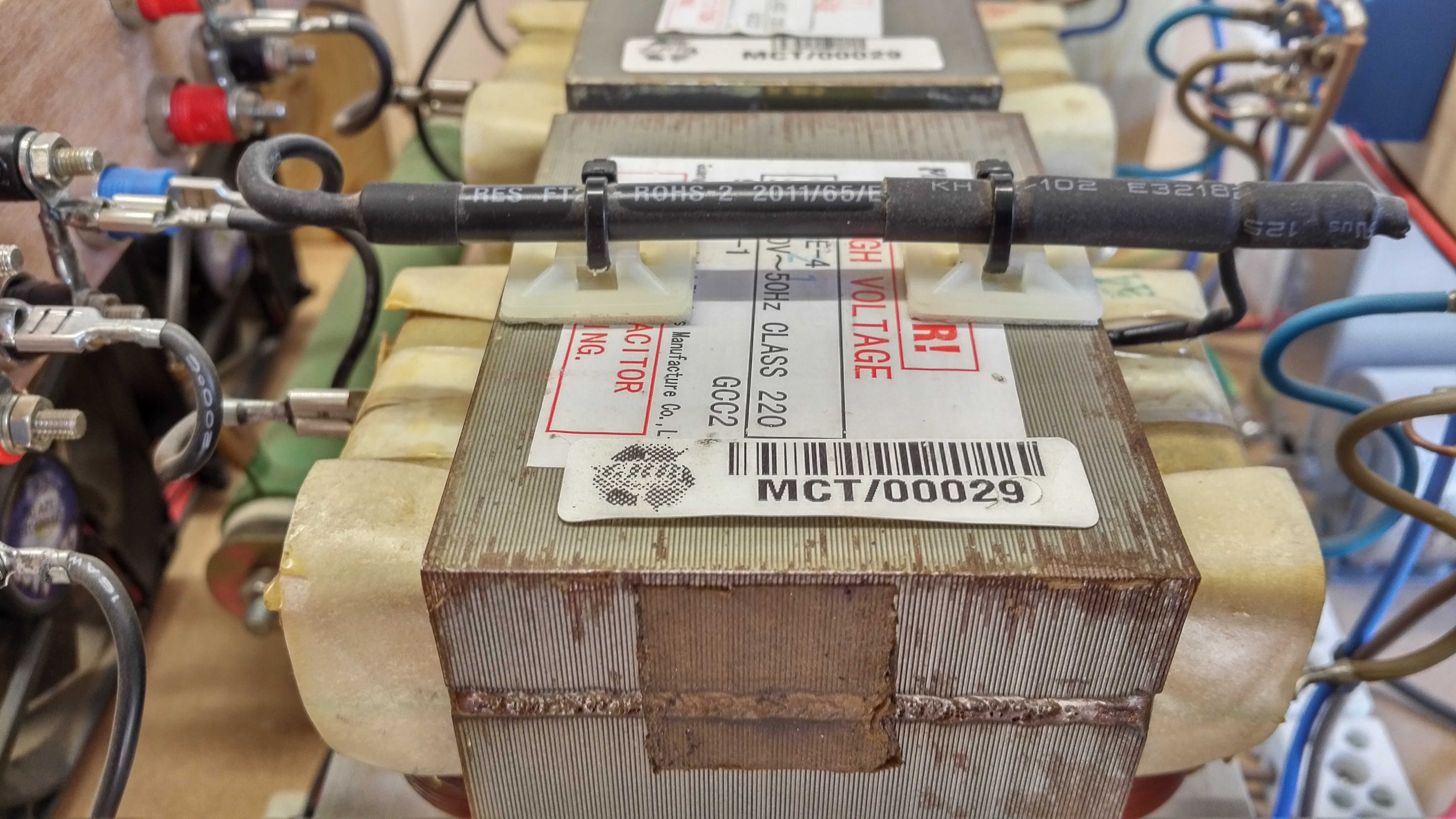
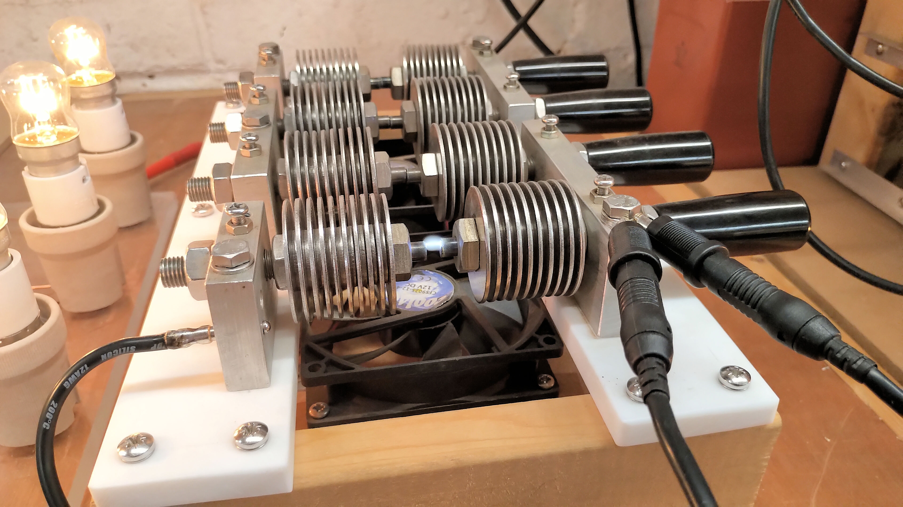
Fig. 1.1. High voltage base unit showing transformers, control circuits, and various different outlets (high voltage, mains, and low voltage).
Fig. 1.2. Three microwave oven transformers (MOTs) can be used individually, or connected in series, or in parallel.
Fig. 1.3. The SCR power controller for the MOTs has been modified to use a long-wire remote control for on-off and power level.
Fig. 1.4. High voltage transformers are cooled when required by twin cooling fans, and a mains bulb indicates power supplied to the primary of the transformers.
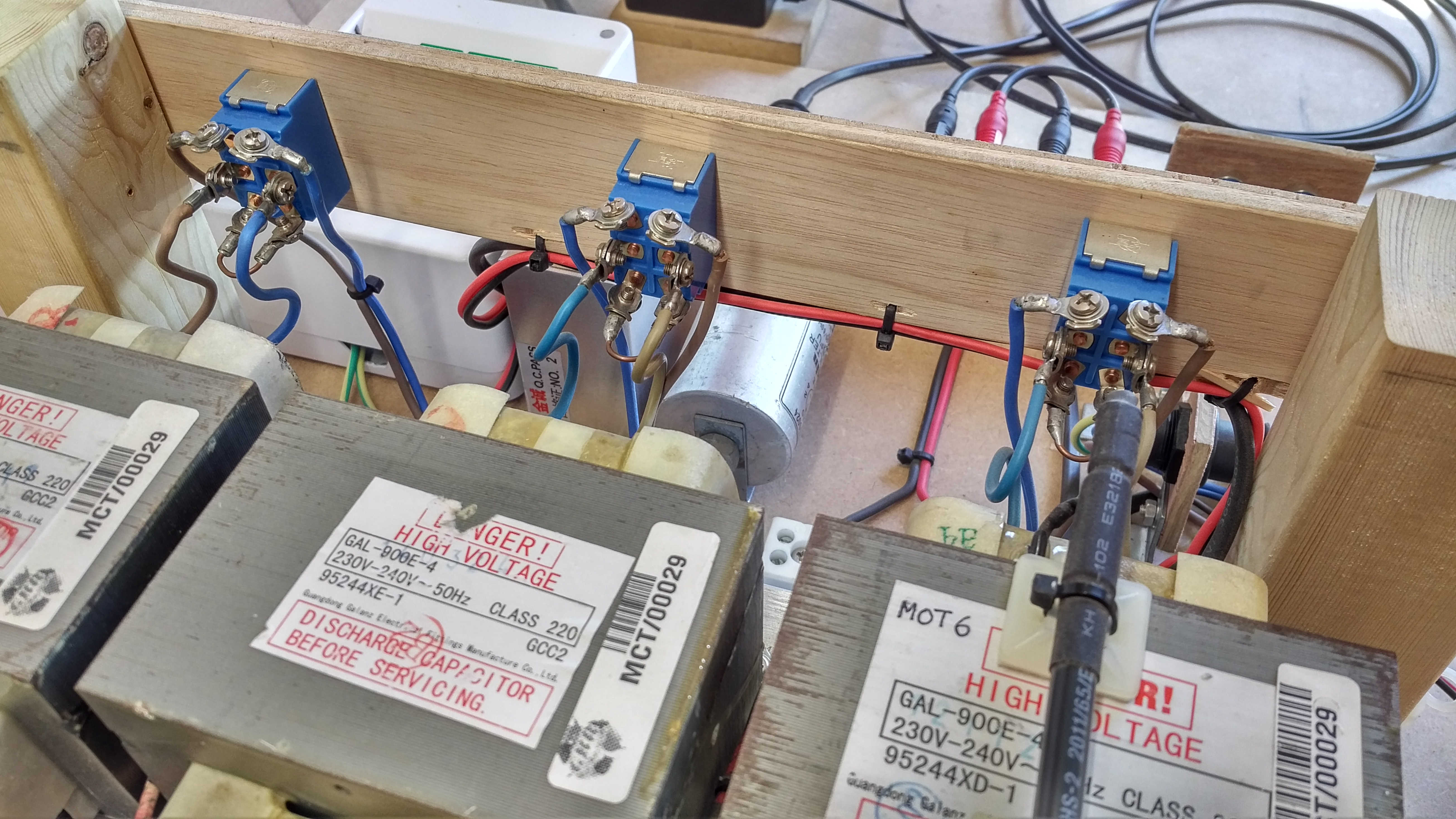
Fig. 1.5. The MOTs are individually switched on-off. The left two are connected in series via their metal core, whilst the right one is isolated from its metal core.
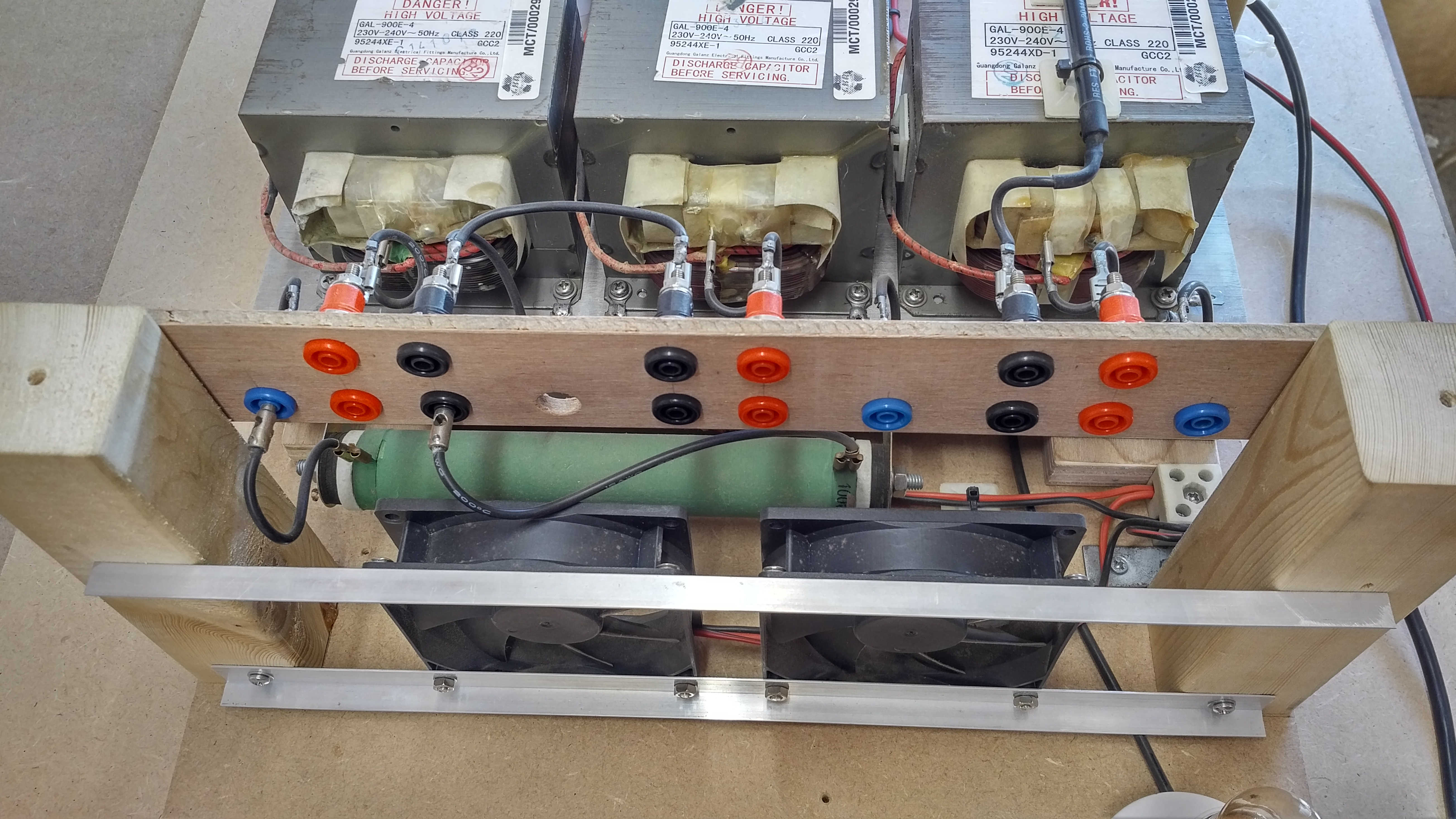
Fig. 1.6. All transformers are mounted on a large metal heatsink, and fan cooling is required for long operating runs at output powers > 500W.
Fig. 1.7. AC mains input power is passed through circuit breakers, filtered, and then fed to SCR power controller.
Fig. 1.8. The remote control allows distance operation of on-off and power adjust from zero to maximum, whilst working directly with the experiment at hand.
Fig. 1.9. The MOT is isolated from its metal core by detaching the core connected end of the secondary, and then routing the connection via high voltage cable to the output connectors.
Fig. 1.10. The two left hand metal core connected MOTs have their primaries connected in anti-phase to allow series connection of the secondaries.
Fig. 1.11. High power load resistor 100Ω @ 100W provides a stabalising load for the transformers when driving high impedance experimental loads.
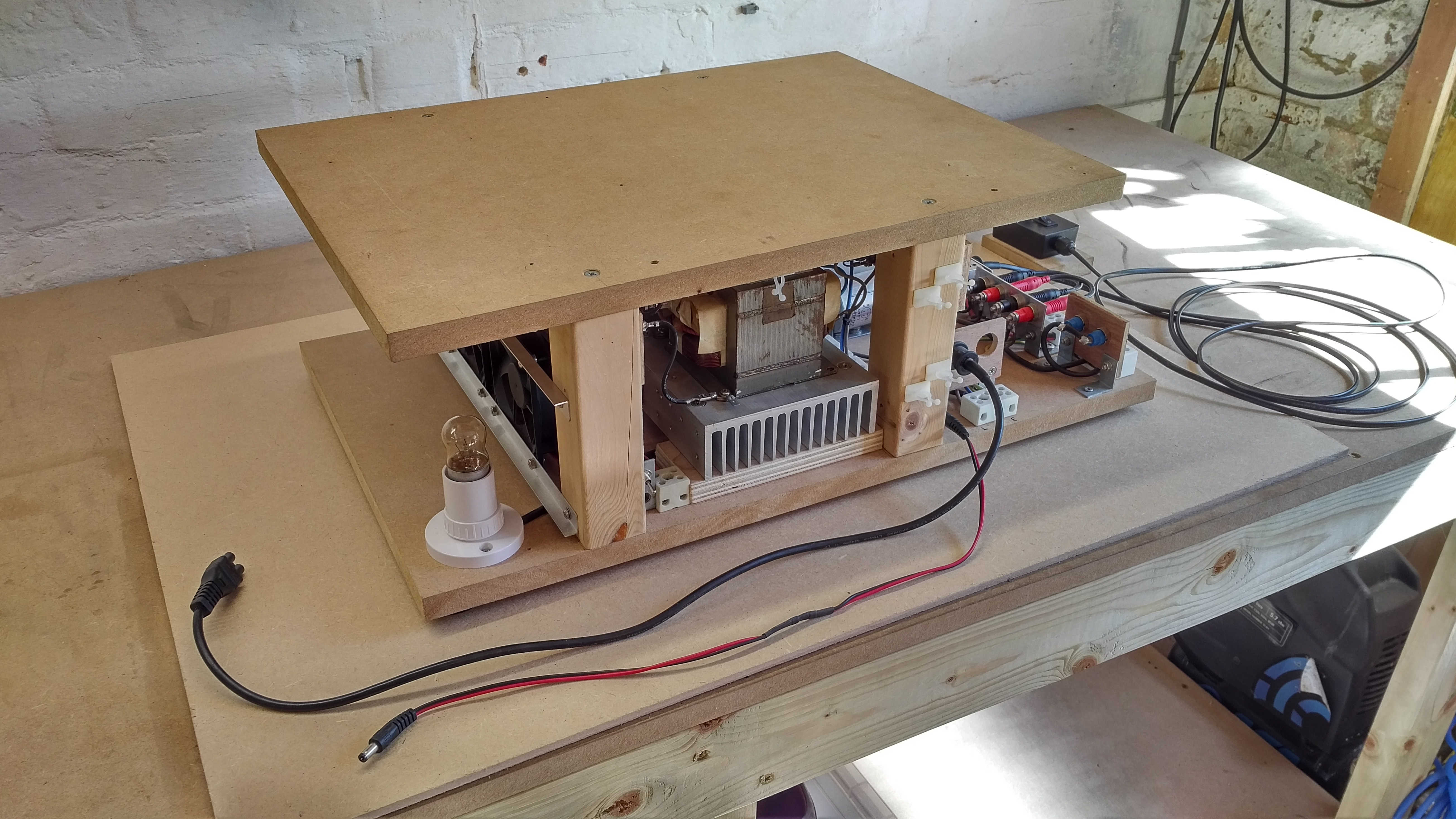
Fig. 1.12. The high voltage supply with mounted upper deck to support generator apparatus.
The circuit diagram for the HV supply is shown in Figure 2 below, or click here to view the high resolution version. The schematic should be referenced for the subsequent circuit description:
Fig. 2.1 High voltage supply schematic showing the supply input stages, remote control, and the transformer output stages.
AC line power at UK standard 240V 50Hz is fed via a high current (16A) 3-pin connector to a domestic distribution box with 3 circuit breakers at 6A, 10A, and 20A. The 6A circuit breaker feeds a low voltage switched-mode power supply unit providing 15V @ 3A and is used to power low voltage circuits in the HV supply and the generator stage including, pre-amplifiers, fans, control electronics, measurement devices, indicators, meters, and any other low voltage units. The HV supply is arranged with a number of low voltage two-pin power jack sockets to supply low voltage generator stage requirements on the upper level. The 10A circuit breaker powers filament transformers for vacuum tube generator stages, and auxiliary devices requiring line voltage AC, via a suitable mains output connector in the form of shielded 3-pin connector, and ceramic connection block for ad-hoc connections. The 20A circuit breaker feeds the high voltage transformers via a suitable power controller.
The distribution unit also has space for an incoming line RCD breaker, but has subsequently been removed, as it was found to be too sensitive to some experiments where power is reflected back into the HV supply, and causing the RCD to cut the power during the experiment. As an alternative a larger RCD was incorporated into the mains distribution for the laboratory, and separate mains circuits fed via a UPS (uninterruptible power supply) to measurement and test equipment, and computers. This arrangement prevents sensitive equipment from inadvertently being switched-off and/or rebooted during certain experiments when the lab RCD would disengage to protect the input supply. Having the test equipment running under these circumstances has proved key to understanding conditions and events within the experiment that have caused large reflections back through the mains supply.
The 20A circuit is first passed through a high current line filter which is used to prevent higher frequency electrical disturbances from being reflected back into the mains supply, and offer a measure of isolation between the two. The output of the line filter is fed to a power controller which enables the variable control of power supplied to the high voltage transformers. This HV supply was specifically designed around the use of the microwave oven transformer (MOT) as the high voltage part of the supply. MOTs are very readily available, and have proved to be a strong and robust transformer for this type of supply. The transformers used are all Galanz GAL-900E based which nominally produce 2100VRMS @ 900W ~0.45ARMS, and are quite common in UK domestic microwave ovens. The MOT represents a significant inductive load to the incoming AC supply, and uncorrected will reduce the power factor from the ideal 1 to ~0.6. To correct for this and reduce the draw on the incoming supply a power factor correction (PFC) capacitor can be used at the AC line input (after the line filter and before the SCR). A 20µF AC PFC capacitor can be used in order to correct for a single MOT. For 2-3 MOTs being used together this can be increased to 40µF.
The MOT is a transformer designed to drive a specific impedance load, (magnetron via a voltage doubler and tuned with a series capacitor), with the minimum quantity, and hence cost, of copper, and with the cheapest and simplest manufacture methods and components. This leads to certain drawbacks in the transformer characteristics, and most especially saturation of the transformer core when driven open-circuit, or connected to a higher than intended load impedance. The core is cheaply manufactured from steel laminate and then welded together which shorts the laminates out, greatly increasing the core saturation rate when adequate power is not drawn from the transformer. A detailed study of the characteristics of the MOT has been presented by Wokoun[2].
The easy core saturation requires the current to be restricted in the primary coil. This is not easily done directly with a variac, as is usual for variable output control of a transformer, since the core easily saturates at low input primary voltages leading to large run-away currents in the primary, rapid core heating, and ultimately destruction of the transformer from excessive heating, not to mention the dangerous risk of a transformer fire which is very hard to deal with due to extreme heating of the steel core even after the power has been cut-off at the input. Instead the current must be restricted either via an inductive load in the primary circuit, or much better, an SCR power controller.
A suitable simple series inductor is the primary of another MOT, (with the secondary shorted), connected in series with the primary of the MOT to act as the HV transformer. Alternatively the secondary of another MOT, (with the primary shorted), can be connected in series with the secondary of the HV transformer MOT, but more heating tends to occur in this configuration from the higher secondary impedance. The series primary connected MOT was found to limit the output current to a degree, and made adjustment with an input variac possible, with less chance of core saturation, but with however limited overall range of adjustment and suitability to changing load impedance. The advantage however of this first method is that the output of the MOT (not in core saturation) is a complete sine wave. In core saturation the output becomes progressively distorted towards a heavily clipped sine wave. It was concluded that this method of power control would be too limited for the wide range of generators that the HV supply would be driving.
The second and preferred method is the SCR based power controller, (similar to a light-dimmer controller but more powerful), which controls the on part of the sinusoidal cycle, and hence controls the overall power delivered to the transformer, which effectively restricts the core saturation whilst providing variable control of the output power. Suitable SCRs are very easily and cheaply available, and a complete unit with an output power of up to 3kW has been used in the HV supply. The disadvantage of the SCR is that the output is no longer a sine wave, but rather a distorted waveform that represents a small part of the total cycle. This has however provided some unexpected benefit in burst and impulse modes that will be discussed in the generator posts, but suffice to say here that the fast SCR turn-off can create very large voltage spikes in the MOT primary as the field collapses, which in turn produces strong impulses in the secondary at the line frequency. These impulses in the secondary, when fed directly to the experiment without a capacitor tank circuit, acts as one method of generating a non-linear trigger for a displacement event.
When working directly with the experiment at hand it is not convenient to keep walking backwards and forwards to the power supply to adjust power level or turn on or off the supply. To enable more distant control of the SCR the variable resistor used to control the power level was removed from the SCR circuit, and positioned in a small plastic box along with an on-off switch. The control box was then attached to the SCR via a long two-wire mains lead (5m), where on-off function is created by switching a higher resistance into the two-wire line, and hence holding the SCR in the off condition, which is also the case if the remote box is disconnected from the SCR power controller. Power control is affected from the variable resistor by reducing the resistance from 500kΩ down to 0Ω, which progressively turns the SCR on for a proportion of the ac line cycle.
Figures 3 below show waveforms from the HV supply at a range of different points in the high voltage supply, and including the high voltage rectifier and tank capacitor at the output to form a load.
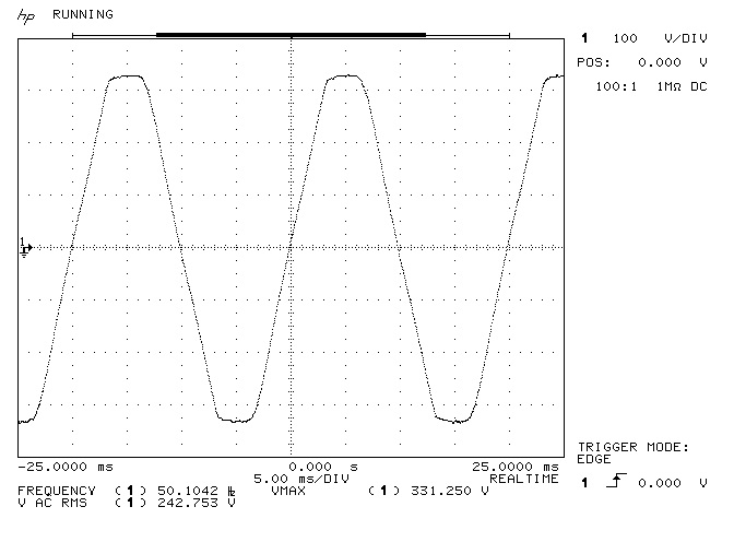
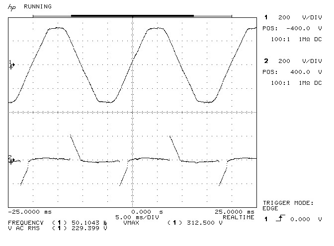
Fig. 3.1 Line input waveform showing badly clipped sinusoidal waveform at ~ 240VRMS and 50Hz (UK standard).
Fig. 3.2 Input (1) and output (2) waveforms of the SCR power controller at 25%, and disconnected from the MOT input.
Fig. 3.3 SCR at 50%.
Fig. 3.4 SCR at 75%.
Fig. 3.2 SCR at 100%.
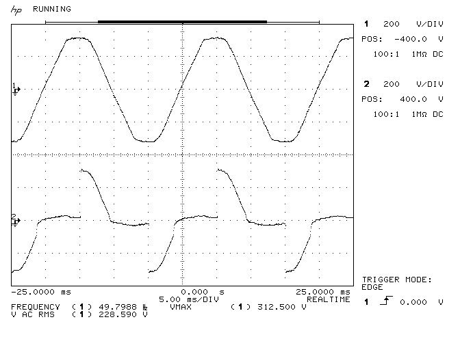
Fig. 3.6 Output of the SCR when connected to a MOT driving a high voltage rectifier and capacitor, and with the SCR set at 75%.
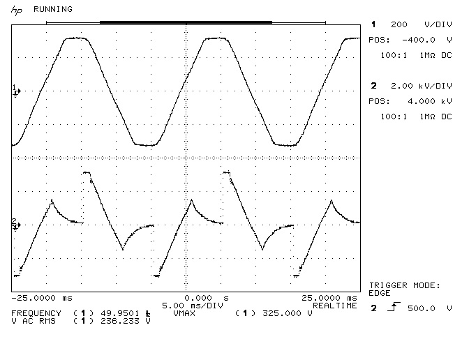
Fig. 3.7 Output of the MOT when driving a high voltage rectifier and capacitor, and with the SCR set at 75% output.
Fig. 3.8 High voltage output from the rectifier and tank capacitor, showing a constant dc voltage at ~3kV.
The output of the SCR power controller is passed through a system of connections to allow the MOTs to either be driven directly from an external source as required, or by direct connection to the SCR. Each individual MOT can be switched independently to the SCR output allowing the transformers to be used individually or combined in parallel or series combinations to increase the available output current or voltage. The output of the SCR is also fed to a 25W mains incandescent lamp which indicates clearly to the operator when voltage is applied to the input of the one or more of the MOTs. This is a simple but important safety factor when working in the experimental environment, and is a rapid but not exhaustive check to the running status of the high voltage supply. It must also always be remembered that considerable energy can be stored in the generator components, such as tank capacitors etc., and that a no visible lamp output is not a direct indication that it is safe to touch any part of the high voltage circuits prior to the appropriate discharge procedures.
The MOT is a cheaply manufactured component with minimum materials and quality, and hence the high voltage winding isolation to the steel core will not usually withstand voltages in excess of ~1.5 times the nominal designed output. This makes it difficult to combine MOTs in series where the core connected terminal of the secondary has been detached from the core in order to float the secondary, whilst keeping the steel core connected to earth for safety purposes. In this configuration the open-circuit peak voltage of the secondary can reach almost ~6kV from 2 series connected MOTs, which can easily arc-over to the steel core through the secondary insulation. When allowed to happen for any period of time the secondary coil is easily permanently damaged.
To overcome this problem and to enable two MOTs to be connected safely in series (both cores earthed), the MOTs are connected in series anti-phase, or center-tapped arrangement. In this configuration the two cores are connected together to earth, which also means the two core connected ends of the two secondary coils are also connected to earth. The primaries of the two transformers are then connected in reverse phase to each other, (as shown in the circuit diagram), such that one transformer produces +VHT out, and the other transformer produces -VHT out. The total output voltage of the series connected secondaries is 2VHT, and the maximum secondary to core voltage on either transformer is only VHT, preventing any secondary to core breakdown.
Of the three available MOTs in the high voltage supply, two are centre-tap connected, and one is floated from the core. This combination was found to be most flexible where the centre-tapped pair are suitable for driving spark gap based generators, and the floated individual is most suitable for driving vacuum tube based generators and if required in conjunction with a diode voltage doubler. In some generator configurations it was necessary to reduce the secondary current using a power resistor, which also in some specific cases helps to stabilise changes in power factor when driving varying or fluctuating high impedance loads from the generator outputs. When and where required a fan-cooled 100Ω 100W wire-wound resistor was used to reduce secondary currents and stabilise the supply output impedance to the next stage. For sustained outputs the MOTs and output components are cooled using a pair of low voltage fans which are manually switched as required.
Overall the high voltage supply has proved to be robust and versatile in providing high voltage in a variety of configurations to a range of different types of generator circuits. The design of the high voltage supply makes it easy to use in the experiments, with accurate and remote control of the output, and constructed with basic and readily available components.
Click here to continue to the 811A vacuum tube generator.
1. Dollard, E. & Lindemann, P. & Brown, T., Tesla’s Longitudinal Electricity, Borderland Sciences Video, 1987.
2. Wokoun, P., Investigations on Using a Salvaged Microwave Oven Transformer, 2003, KH6GRT Website
Negative resistance is a feature of the I-V characteristic of a discharge between two electrodes, and if correctly utilised can lead to unusual electrical phenomena within an electrical circuit. In this first part on this topic we explore the I-V properties of the negative resistance (NR) region of a carbon electrode spark gap (CSG), or carbon-arc gap. When the CSG is biased into the correct region, and combined with a switched (non-linear) impetus from the generator, the impedance of the circuit can be seen to reduce from the conventional short-circuit case, increasing the current in the circuit and intensifying the light emitted from an incandescent lamp load.
The negative resistance characteristics of a spark gap where explored and utilised by Chernetsky[1] in order to demonstrate what he called the self-generating discharge (SGD). The SGD is a state of discharge where he claimed that the energy consumed from the generator was reduced, yet the power dissipated in the load was increased, and where the additional energy in the electrical circuit was “inducted” from the surrounding medium, or what is commonly referred to as the Aether[2], a “gaseous” medium that is all pervasive throughout space, and is also considered to extend beyond the physical realm. As such Chernetsky claimed an over-unity (OU) phenomena where the total output power was greater than that supplied to the circuit by the generator. This experiment has been replicated by others, including Frolov[3], and Dawson[4], who also claim to have measured OU output. This sequence of posts investigates these principles, attempts to measure the claimed OU output, and further explore its possible origin. Ultimately the studied phenomena forms part of the continuing central research, of revealing the inner workings of electricity, and hence the displacement and transference of electric power.
When investigating over-unity claims good experimental and scientific method is critically important. I have found many situations where OU has been attributed to unusual phenomena without being supported by good and well measured experimental data. OU most often appears to arise in non-linear systems, which owing to their transient nature are also difficult to measure reliably, especially when output power is to be accurately measured. Input power is usually quite straight-forward to measure accurately as it is supplied by dc sources such as batteries and power supplies, or drawn from the mains utility supply which is a low-frequency sinusoidal input. In these cases electrical instruments can be arranged to accurately determine real and reactive input power.
Where the generator produces a non-linear output through switching, pulses, impulses, or chopping an otherwise dc or low-frequency sinusoid the dissipated output power can become a complex transient, with many high-frequency components, and many different phase relationships within the experimental circuit. When this is combined with high voltage and/or current magnification , multi-resonant elements, different transmission modes both transverse and longitudinal, cavity and termination effects, and hence significantly changing boundary conditions on the dielectric and magnetic fields of induction, the final accurate determination of output power, even with sophisticated instrumentation, is exceedingly complex, and can very easily lead to substantial errors and mis-understandings. As such, and due to the complexity of these measurements, the phenomena themselves are easily attributed to OU directly without further detailed assessment, and videos show the qualitative results of the phenomena without significant quantitative supporting evidence. It is not surprising given the often lacking experimental method, and lack of detailed supporting measurements, that conventional science so often holds a cautious and pessimistic view of the OU field.
Having stated this, OU is a very important exploration into the unknown, in the search for a truly sustainable, re-generative power source, and one that attracts wide and diverse forms of research and endeavour. My own research is orientated towards revealing the inner workings of electricity, and through co-operating with life’s natural processes, reveal the re-generative and inclusive nature of these under-lying processes. In this sense my own research strives for best scientific method, and well quantified supporting measurements, which then make it possible to either refute or support established claims, whilst making it possible for me to venture new claims of my own as to the origin, principle, and mechanisms of the explored phenomena. Often one experiment leads to another, as in the case of the experiment that is presented in this post. Whilst interesting phenomena are observed, explored, and measured, further experiments will be required to validate Chernetsky and others’ claims, that the additional energy in the OU experimental system is induced from a medium external to the electrical circuit. In my experiments in this post I find the additional energy that intensifies the luminance of the load, is drawn through the generator from the line supply, and directly as a product of biasing the CSG to utilise the NR properties in the abnormal glow region of the discharge.
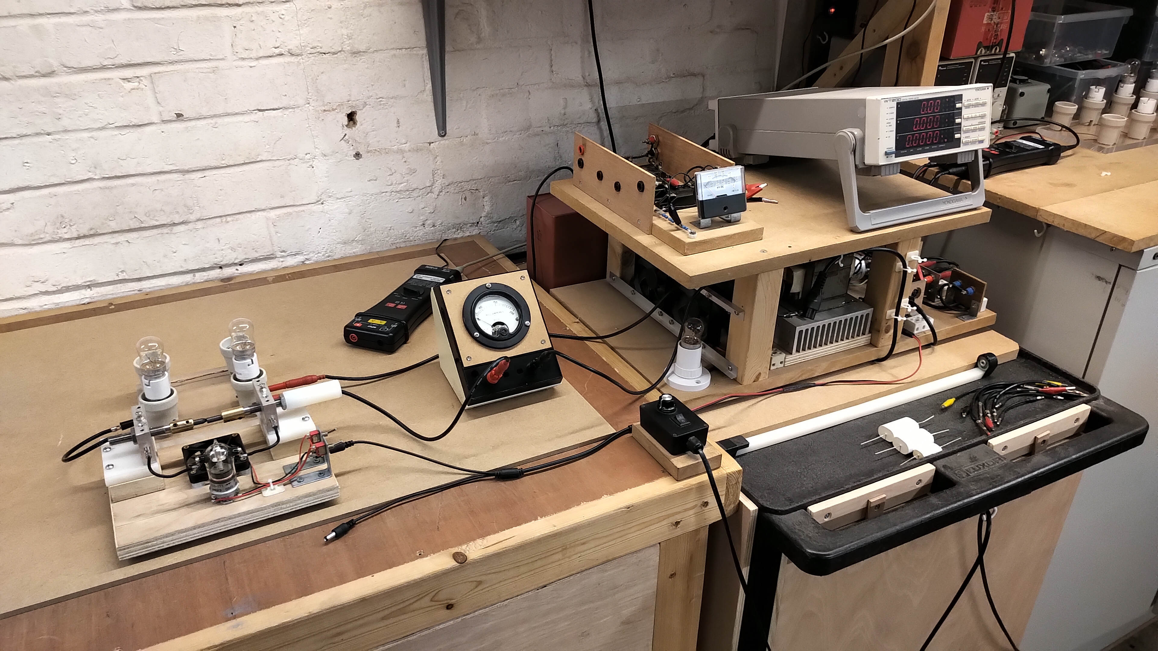
Figures 1 show the experimental apparatus and circuit, and some of the different types of measurements taken as part of the experiments.
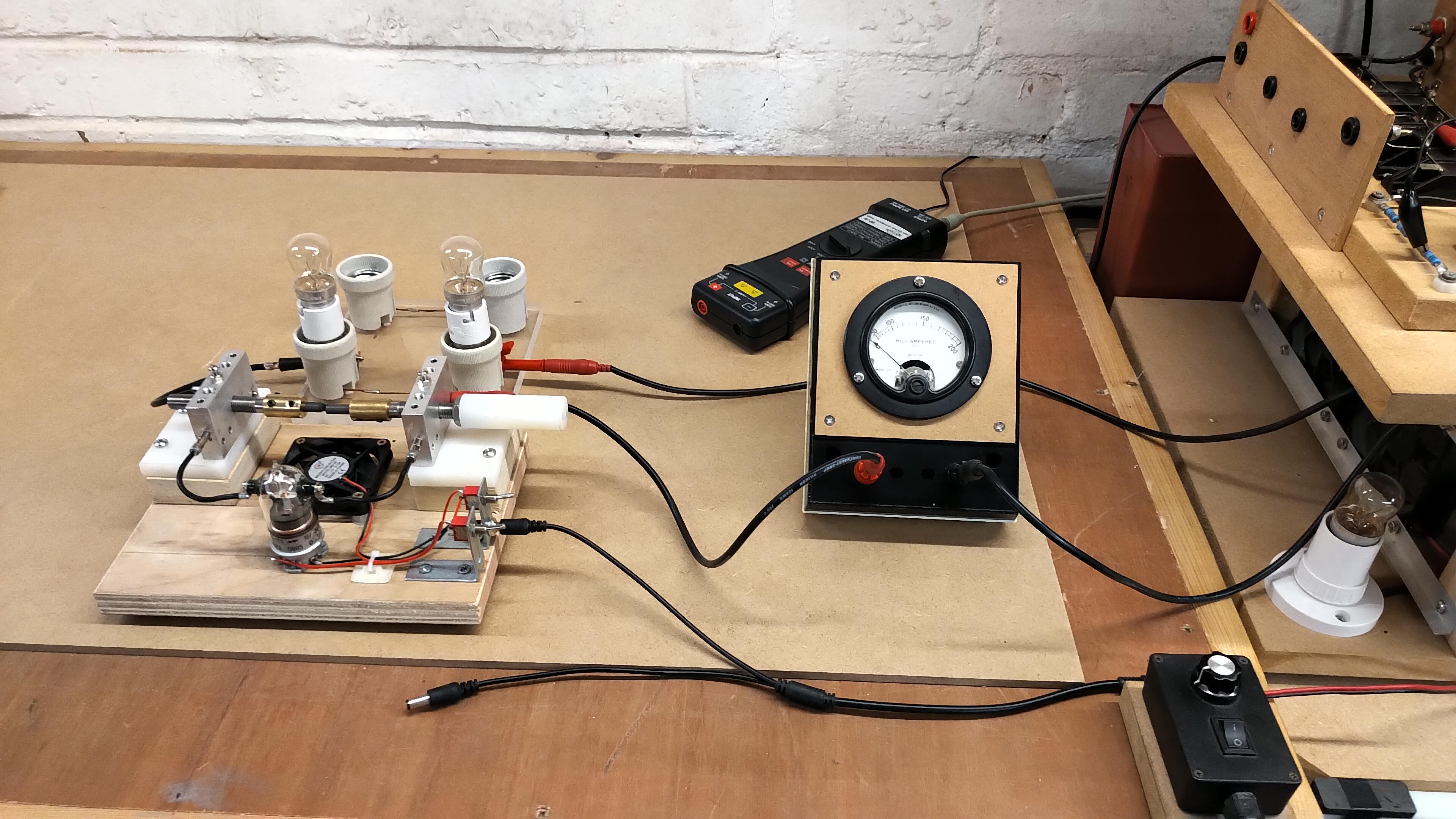
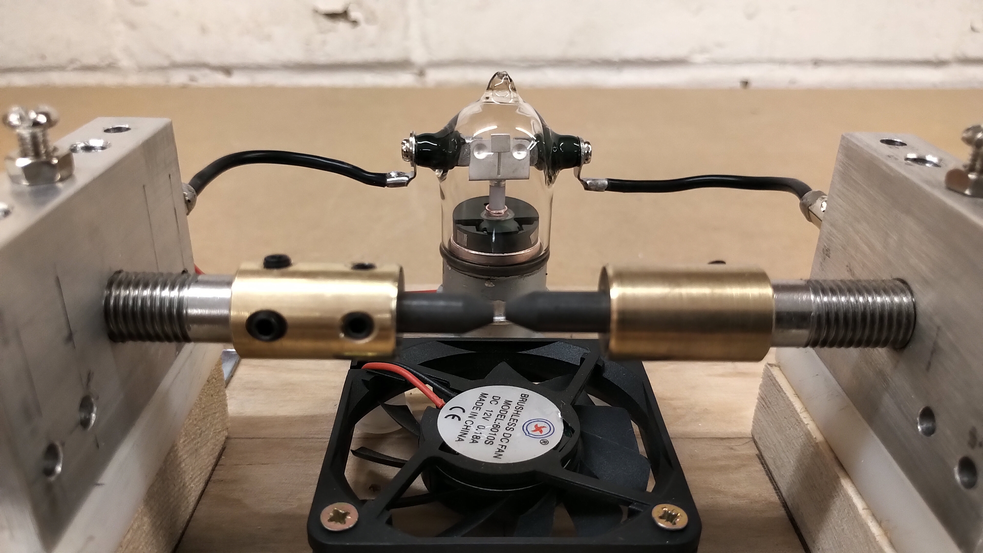
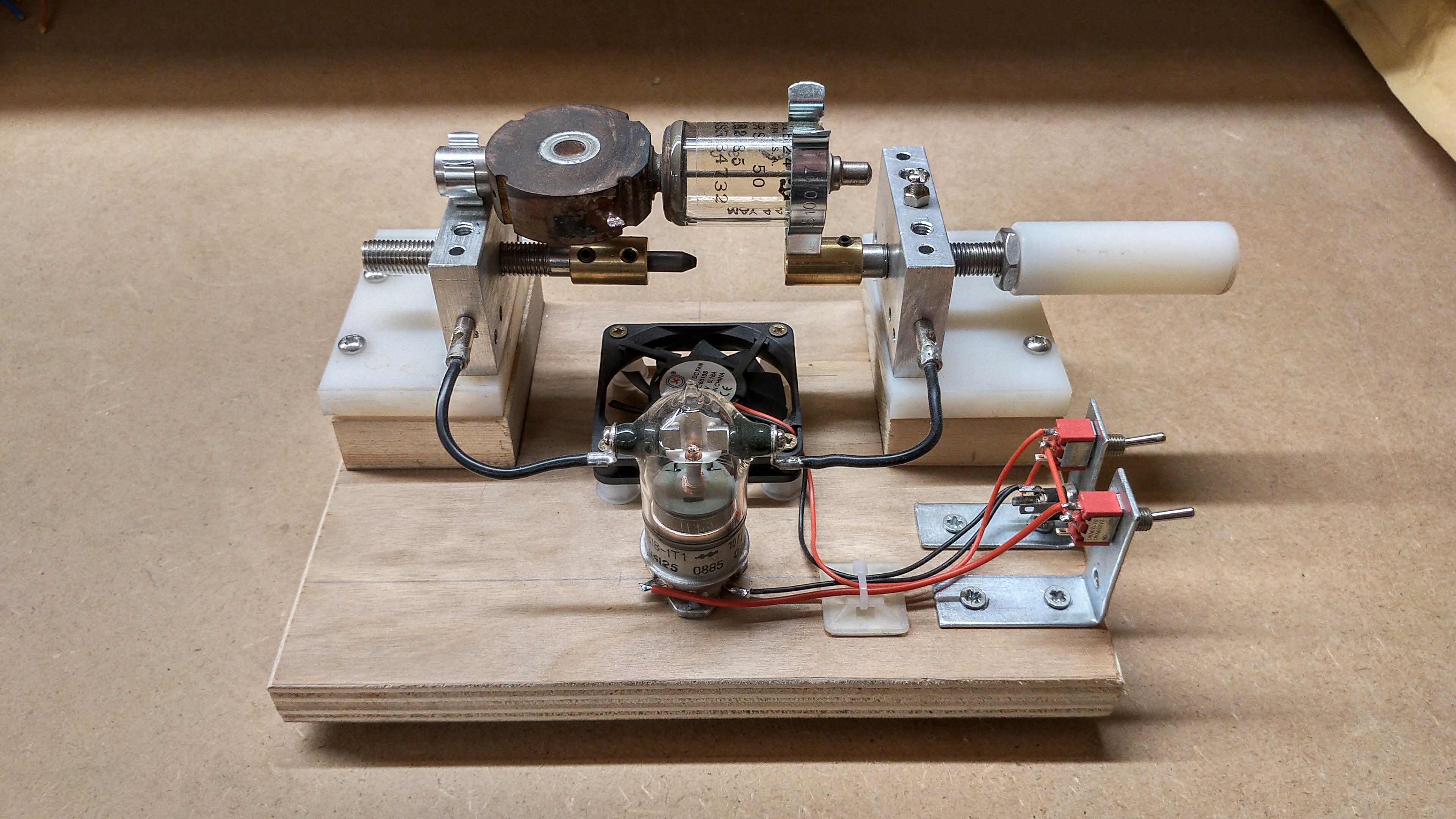
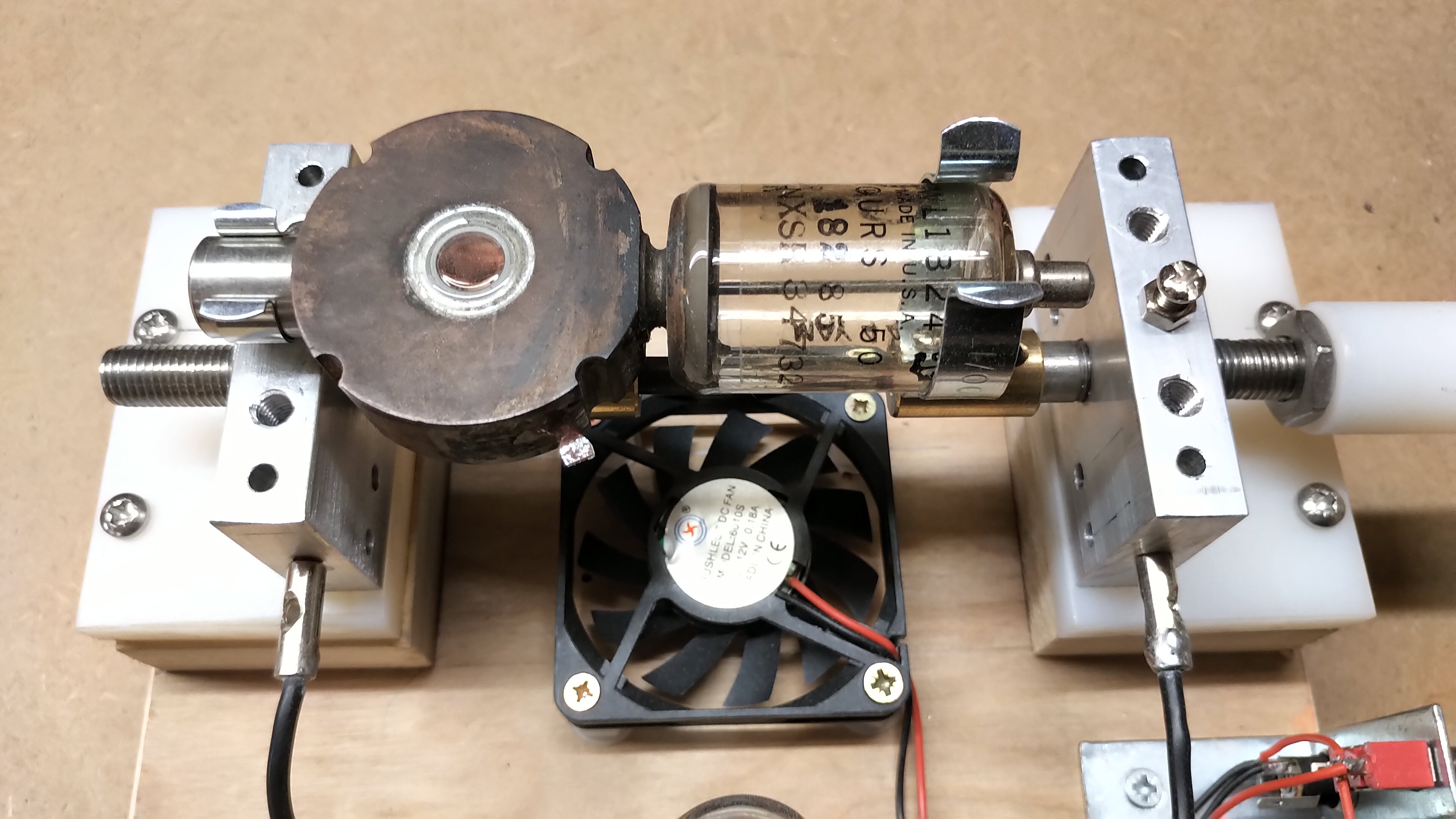
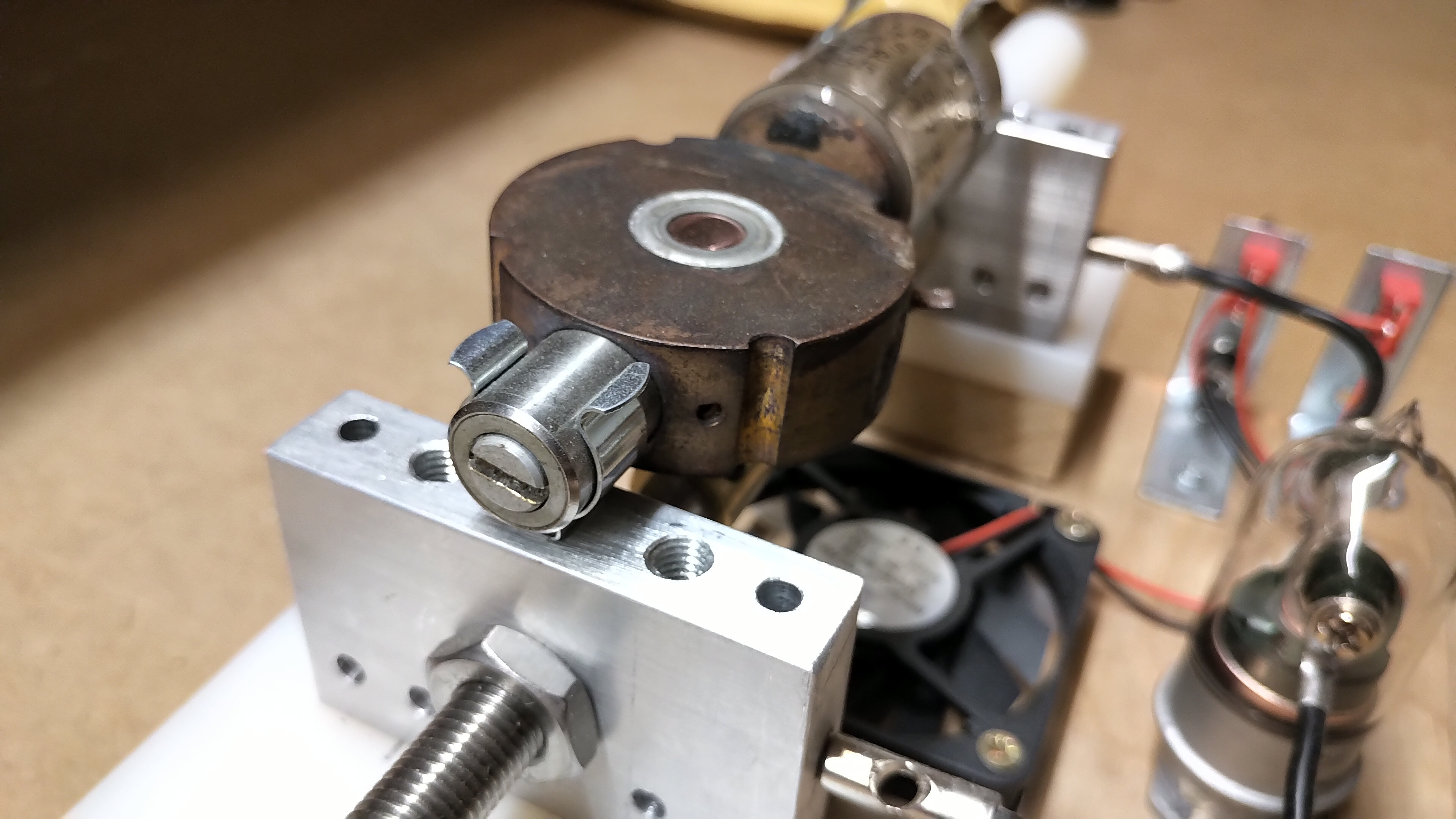
Fig. 1.1 The complete experimental setup including the HV supply and rectifier, Yokogawa power meter and rf ammeter, carbon arc spark gap (CSG), and the incandescent lamp load.
Fig. 1.2 The 200mA RF thermo-ammeter is used to monitor the rms current in the experimental circuit. Non-linear transient drive from the generator is necessary to utilise the negative resistance region of the CSG.
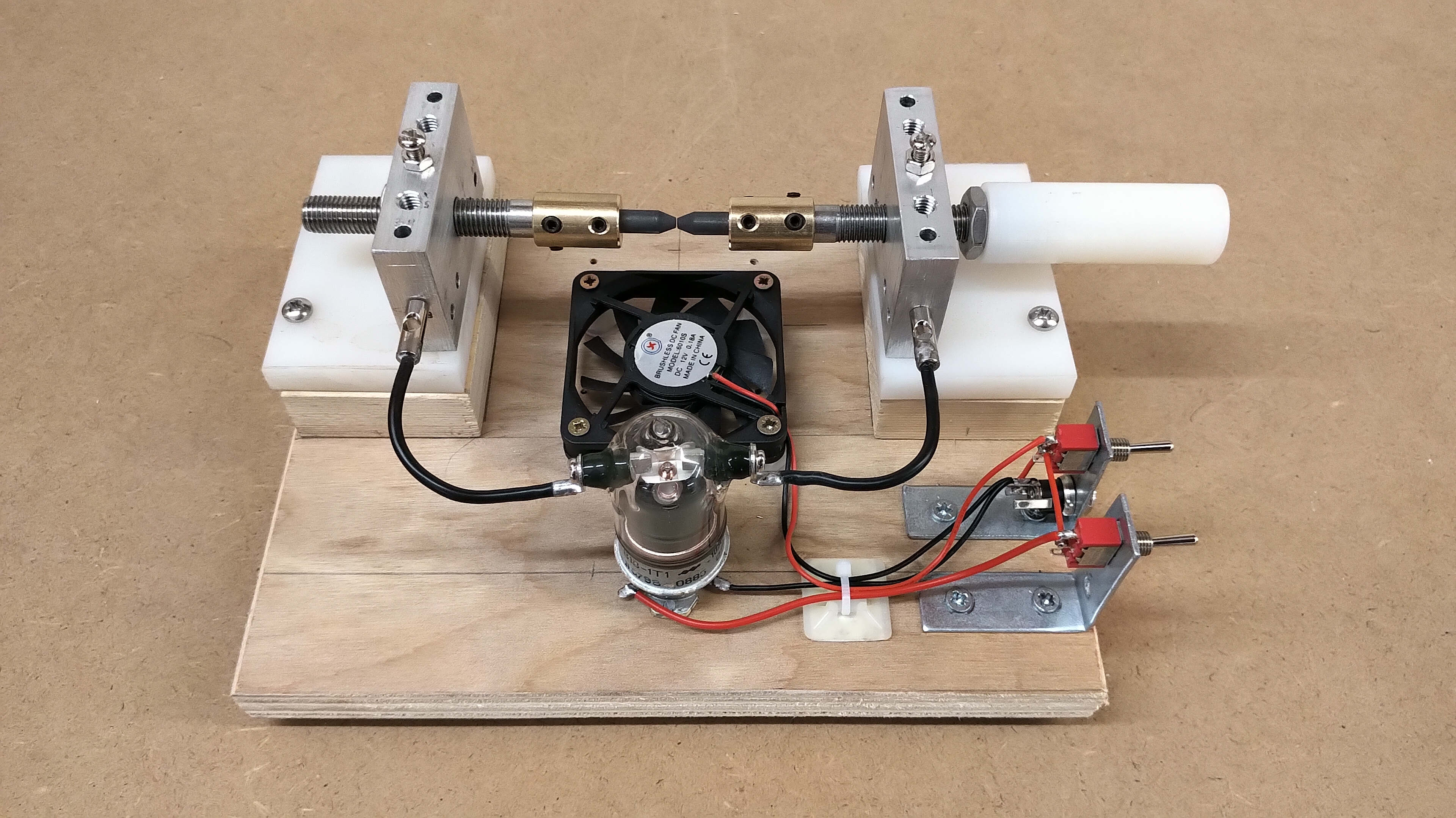
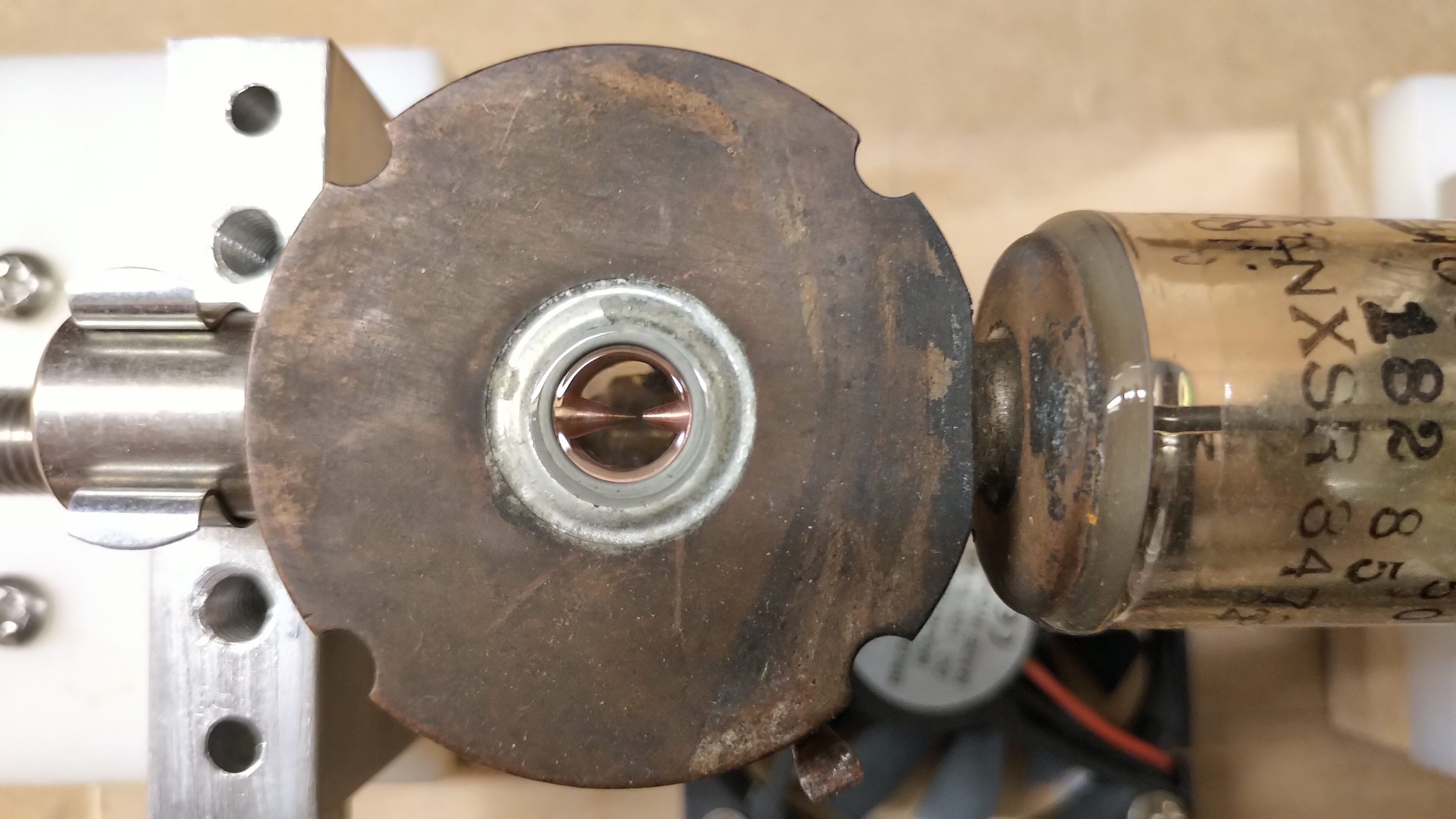
Fig. 1.3 The carbon electrode gap size can be adjusted using the nylon handle during operation. The gap is shunted by a B1B 3kV 10A vacuum relay operated from the DC 15V supply. Fan cooling of the carbon electrodes can also be used for plasma arc experiments.
Fig. 1.4 The vacuum relay provides a short-circuit path across the electrodes for circuit impedance measurements and comparison. When switched off conduction in the circuit is via the I-V characteristics of the CSG.
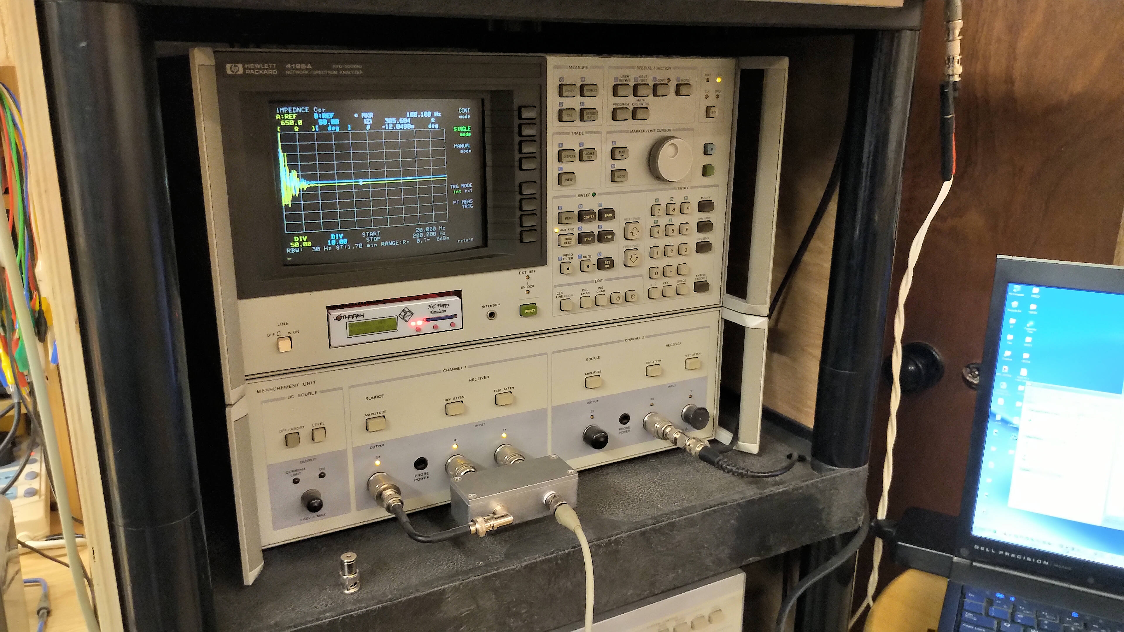
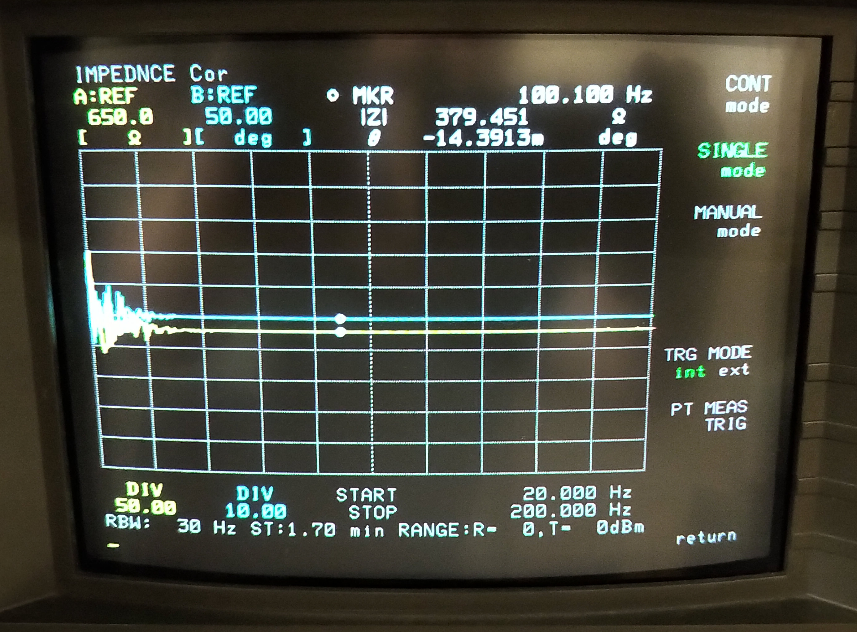
Fig. 1.5 The low frequency input impedance Z11 from the perspective of the generator, measured using the HP4195A, and showing a linear resistive impedance over the range 20-200Hz.
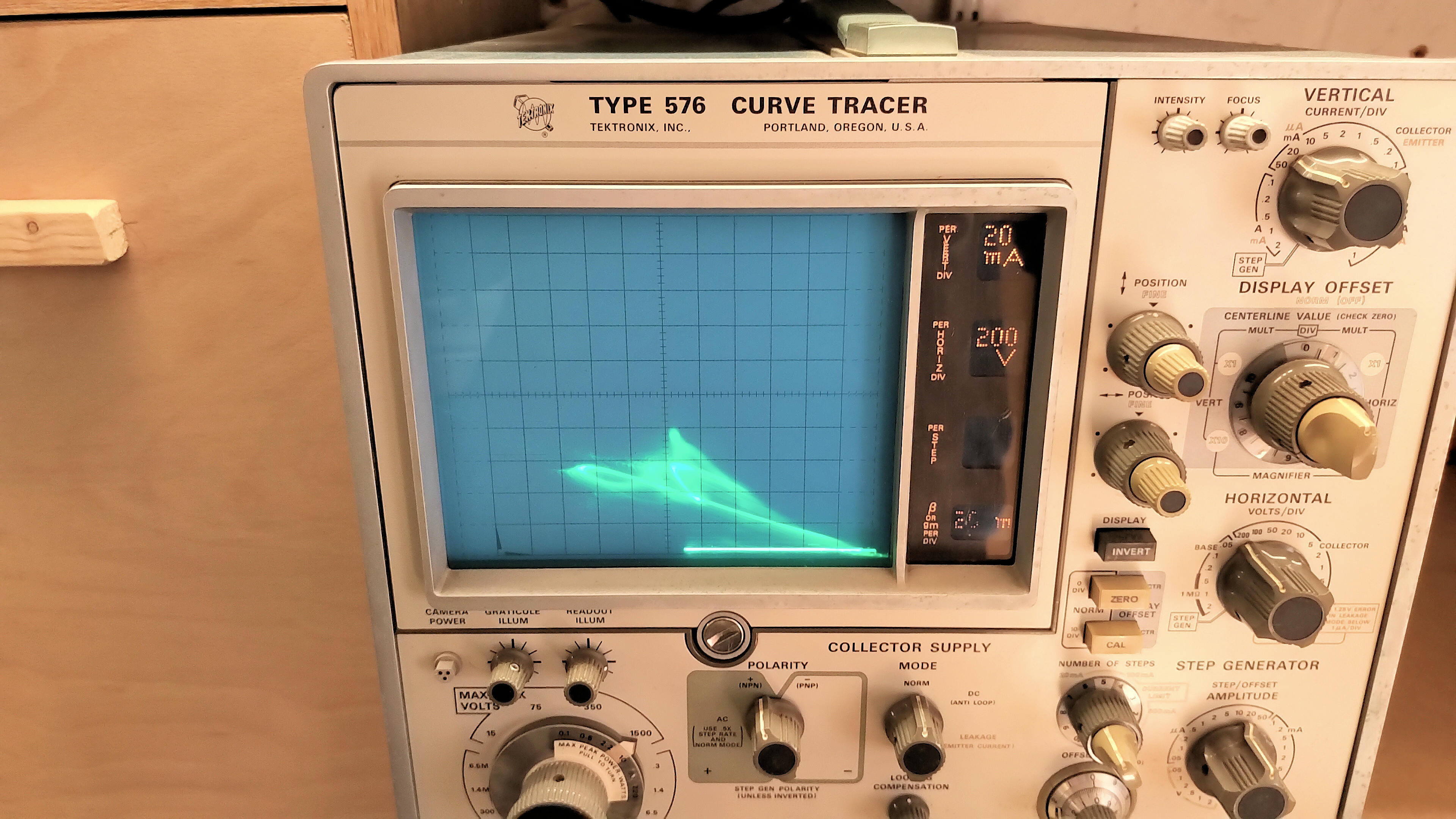
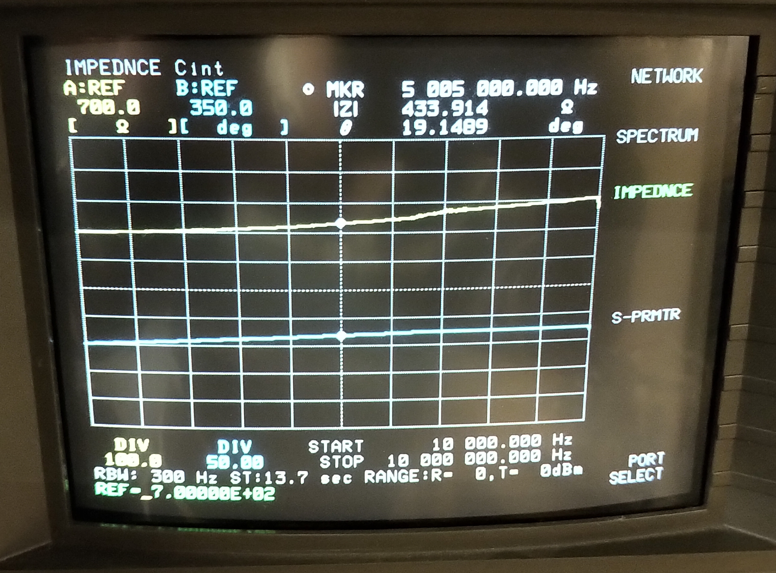
Fig. 1.6 The I-V characteristics of the CSG as measured by a Tektronix 576 curce tracer, with the measurement power limited to 10W. Here the CSG is biased into the negative resistance region prior to the onset of arc discharge.
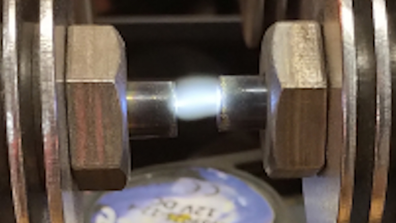
Fig. 1.7 An adaption of the experimental circuit using a single tungsten electrode spark gap, and showing the white plasma arc developed over a gap of ~ 5mm.
Fig. 1.8 A closeup view of the silent white hot plasma arc developed in the gap when switched with a non-linear transient drive. The white beam of the discharge and its surrounding halo extend over ~ 5mm electrode gap.
The generator for this experiment is a single HV transformer in the High Voltage Supply (HVS), the output is rectified and connected directly to one electrode of the CSG via an RF ammeter, (Weston 425 200mA FSD). The other electrode of the CSG is connected to a two lamp series incandescent load (2 x 25W = 50W) and then back to the other terminal of the HVS transformer. The CSG has fan assisted cooling, and is shunted in parallel by a 3kV 10A vacuum relay, which enables the CSG to be switched in and out of the circuit for impedance and load power comparisons. The fan and vacuum relay are driven by a low voltage 15V output provided again by the HVS. The input power to the HVS transformer is continuously measured using a Yokogawa WT200 Digital Power Meter.
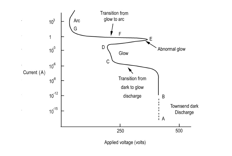
The process of ionisation in the region between two electrodes with a high electric field, is well studied in the prior art[5]. Liberated electrons within the discharge region are accelerated by the electric field between the electrodes, and in the process of moving towards the anode cause further ionisation of atoms, leading to an electron avalanche effect known as a Townsend discharge. Figure 2 below shows the typical current-voltage (I-V) characteristics for a Townsend discharge transposed from Abdelrahman et al.[6]. The negative resistance characteristics utilised in this experiment result from biasing the CSG to the correct region of this I-V curve, around the abnormal glow region between points D-E-F-G . The interesting and unusual phenomena presented in this experiment result from the reduction in circuit impedance, when the biased CSG is combined with a suitable load circuit (incandescent lamps), and driven from a non-linear transient high voltage generator at the line frequency.
Fig. 2 A typical current-voltage (I-V) characteristics for a Townsend discharge between two electrodes. The negative resistance phenomena explored in this experiment result from biasing the CSG around the abnormal glow region, between points D-E-F-G.
The following video introduces the apparatus, experiments, and phenomena associated with the negative resistance of a CSG, and demonstrates aspects of the following:
1. A qualitative observation of the discharge produced in the CSG when biased into different regions of the I-V characteristic, including open-circuit, short-circuit, abnormal glow (D-E-F), and arc discharge (G) regions.
2. Adjusting and biasing the spark gap into the abnormal glow region to utilise the negative resistance properties within the electrical circuit.
3. The change in impedance of the circuit when switched between short-circuit conduction and spark gap discharge.
4. The change in circuit current and dissipated power in the load with switched impedance, and the effect on the input power to the generator from the line supply.
5. A comparison of adjusting and biasing the circuit when driven from a non-linear transient input, and a linear sinusoidal.
6. Measurement of the generator output using an oscilloscope both in the non-linear and sinusoidal cases, and showing the switching transients generated when the CSG is biased into the negative resistance region.
7. An experimental investigation of the I-V characteristics of the CSG using a Tektronix 576 curve tracer.
Figures 2 below show in detail some of the additional measurements made during the experiment including the overall impedance properties Z11 of the experimental circuit from the perspective of the generator, the different drive conditions applied from the generator, and the NR characteristics of the CSG measured on the Tektronix 576 I-V curve tracer.
Fig. 3.1 The low frequency input impedance Z11 for the experimental circuit with the vacuum relay on as a short-circuit across the CSG. The resistive impedance is dominated by the cold resistance of the lamp loads.
Fig. 3.2 The HF input impedance Z11 of the experiment up to 10Mc. The low frequency resistive impedance increases due to inductance of the cables in the circuit, and with no self-resonant properties in the band.
Fig. 3.3 The input to the HV transformer at the SCR output (green), and the output of the HV rectifier (yellow). The SCR creates a switched non-linear pulse drive to the experiment.
Fig. 3.4 The CSG is adjusted to utilise the NR region of the I-V characteristics. Impulse currents from discharges in the CSG are present, along with an increase in peak voltage at the HV rectifier output ~1.8kV.
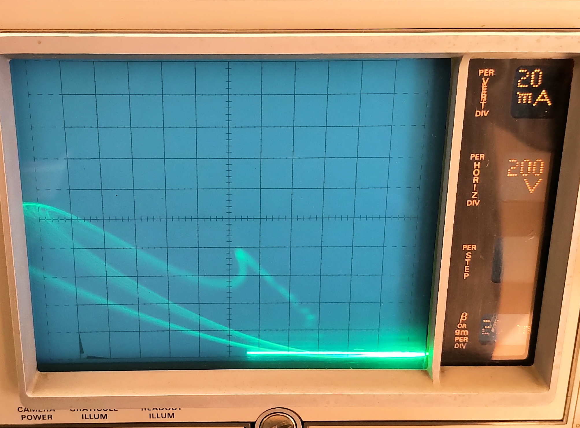
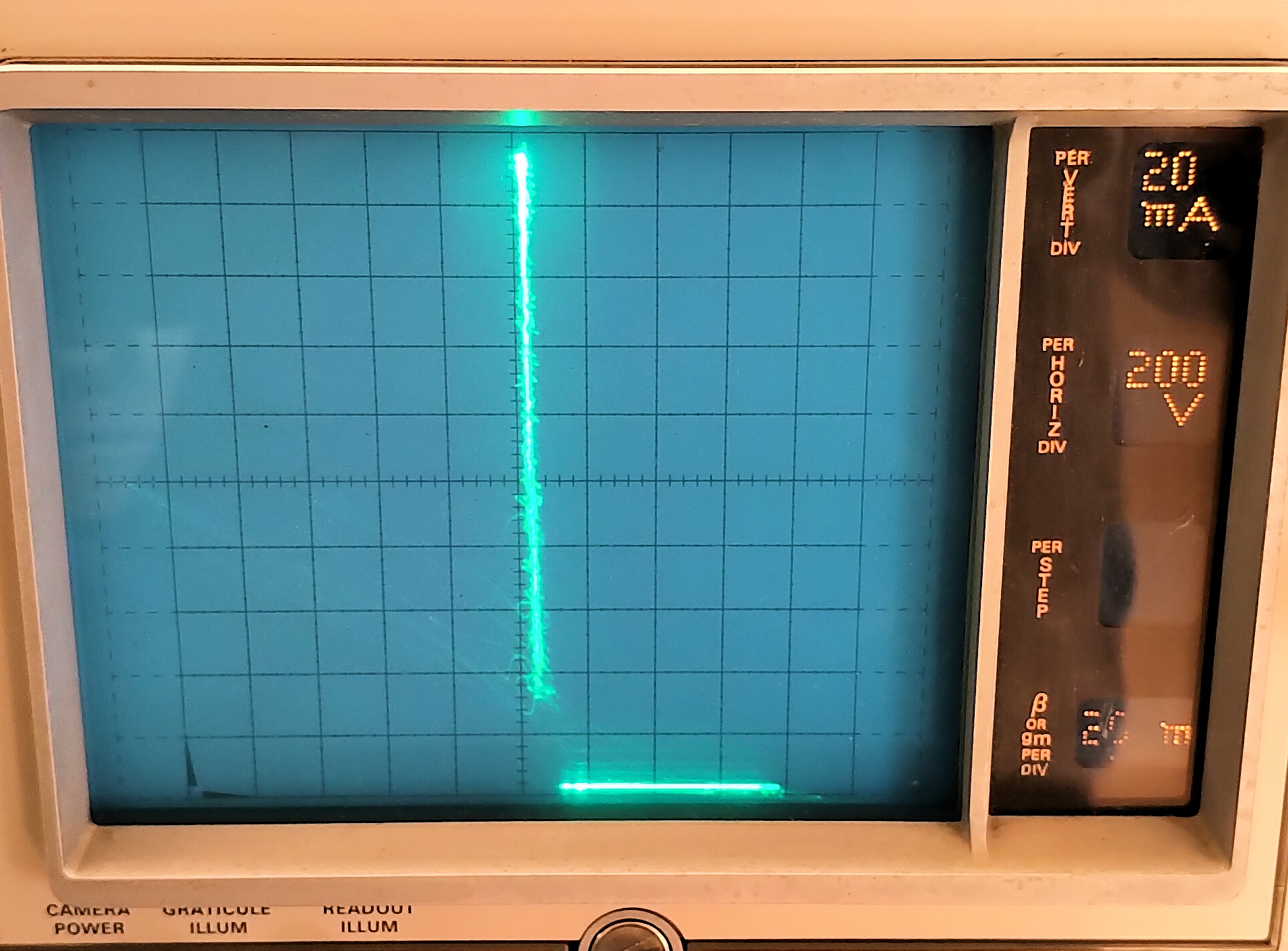
Fig. 3.5 I-V characteristics of the CSG on a Tektronix 576 curve tracer. The output power of the tracer is limited to 2.2W @ 1500V. In the NR region the trace rapidly sweeps negative in a wide arc before coming back toward the centre bias point at around 80mA.
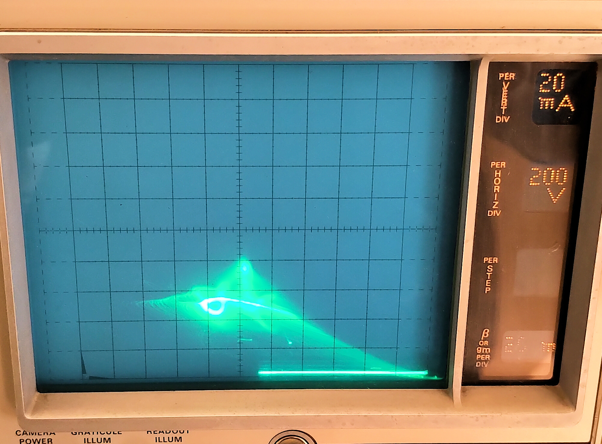
Fig. 3.6 Tracer output power limit 10W. At 1200V the transition to the NR region is reached. The transition is quicker with less magnification to the left of the screen, and a tighter and more direct path to the centre bias point.
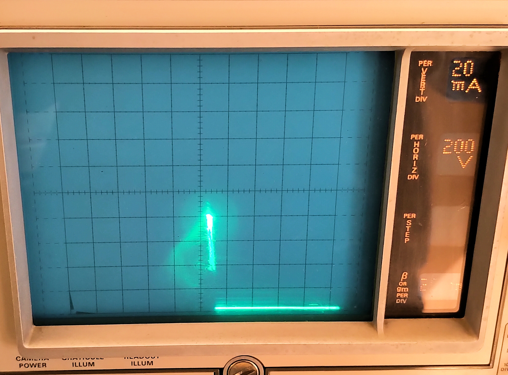
Fig. 3.7 Tracer output power limit 50W. The loops of the NR region are just visible, and show how rapidly the onset of arc discharge occurs when the circuit current is less restricted.
Fig. 3.8 Tracer output power full 220W. The wide arcs of the negative resistance region are just visible, but the transition through this region is very rapid. The arc discharge is fully developed in region G+ (Fig. 2).
To view the large images in a new window whilst reading the explanations click on the figure numbers below:
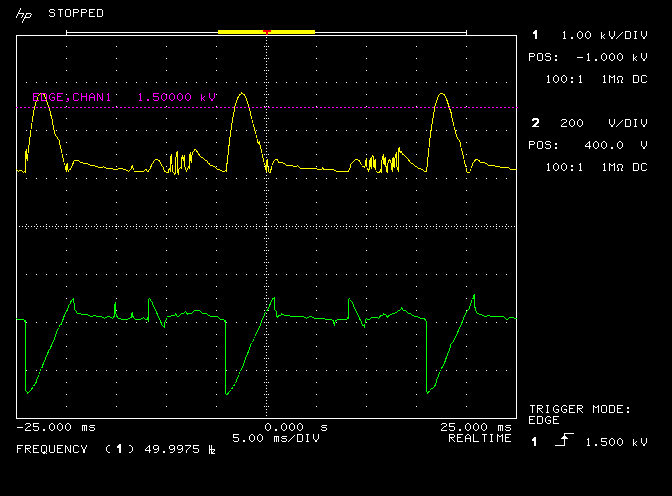
Fig 3.1. Here we look at the low frequency small signal input impedance Z11 from the perspective of the generator, using the HP4195A network analyser. The circuit was measured and compared in two conditions, firstly with the carbon electrodes touching at the ends forming a short-circuit, and secondly with the electrodes parted and the vacuum relay activated to shunt the electrode gap with a short-circuit path through the relay. In both of these cases the impedance measured was the same in magnitude and phase and shows that above 25Hz and up to 200Hz the circuit is completely resistive at a constant 379.5Ω, and constant phase of ~ 0° (-14.4 mdeg @ 100.1Hz). Below 25Hz will also be a continuous constant resistive impedance but requires considerably reduced resolution bandwidth to remove the measurement noise observed. A reduced resolution bandwidth in this case represents a considerably increased scan time for the measurement. This measurement shows that there are no unusual impedance characteristics at the base drive line frequency, no resonant characteristics, and that the circuit appears as a constant resistive load that results almost entirely from the cold resistance of the incandescent lamp filaments, 2 x 25W in series, (in the range 175 – 200Ω each).
Fig 3.2. Shows the HF small signal input impedance Z11 from the perspective of the generator up to 10Mc, using the HP4195A network analyser. The SCR in the HV supply creates a switched output from the incoming sinusoidal line supply, (see Fig. 3.1 here for detailed input and output waveforms), which means there are many higher frequencies present at the output of the HV transformer. This constitutes a non-linear transient drive to the experimental circuit, which is the summation of many higher frequencies, and hence higher frequency characteristics of the circuit impedance contribute to the overall circuit operation, and may play a part in the observed phenomena. This is then combined with the high frequency transient switching in the spark gap itself, which adds a much wider band of available frequencies, and the all important impulse-like currents in and around the abnormal glow discharge region. We can see from this measurement that the resistive impedance rises gradually with frequency reaching ~ 434Ω @ 5Mc, and ~503Ω @ 10Mc. There are no significant features in the measured band, the circuit is not self-resonant up to 10Mc, and the overall circuit is largely resistive with a small amount of series stray inductance from the the wiring.
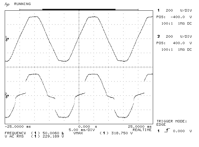
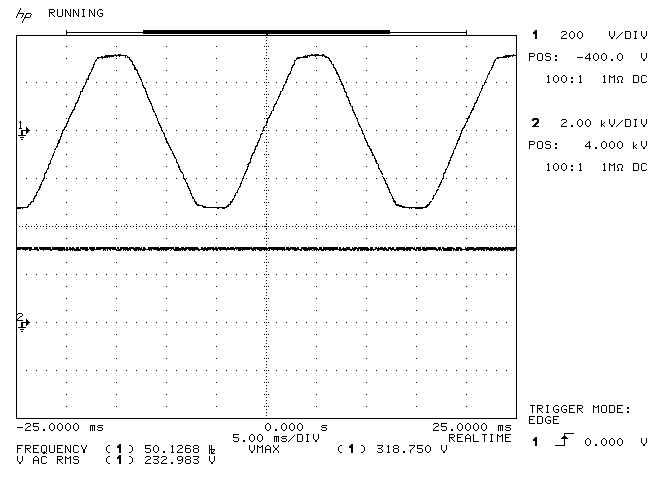
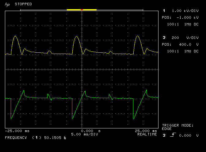
Fig 3.3. Shows the oscilloscope waveforms both for the input to the HV transformer at the output of the SCR (green), and the output of the HV rectifier at the input to the experimental circuit (yellow), where the circuit is set with the vacuum relay closed across the CSG. The SCR output shows how the line sinusoid is chopped into a small section, in this case part of the negative half of the cycle, providing pulses of input current to the HV transformer. The output of the HV rectifier is a voltage magnified pulse train up to ~ 2kV, and set at ~1.3kV peak for this experiment. This output level is sufficient to generate discharges in the CSG, whilst low enough to allow fine control of the I-V characteristics through electrode gap adjustment.
Fig 3.4. Here the vacuum relay has been opened and the CSG adjusted to utilise the NR region around the abnormal glow section of the I-V characteristics. The basic form of the waveforms are the same as in Fig. 3.3 with the addition of some impulse currents from discharges in the CSG, an increase in peak voltage at the output of the HV transformer ~ 1.8kV, and a slight increase in the “on” cycle of the SCR from ~ 4ms to 5ms. This corresponds to increased brightness in the lamp loads, an increased current in the experimental circuit from ~ 100mA to 125mA, and an increase in the power drawn from the line supply ~ 50W to 80+ W. The bias adjustment of the SCR remains the same as for the condition in Fig 3.3, yet clearly by operating the CSG around the abnormal glow region of its characteristics more power is drawn in through the line supply, reflecting a reduction in impedance in the experimental circuit below that of the normal short-circuit impedance at the CSG electrodes or through the vacuum relay. When the experimental circuit is biased at this point the region between the carbon electrodes is mostly dark and visibly discharge free, with the occasional momentary white flash as a discharge occurs across the electrodes when point G (Fig. 2) is reached.
Fig 3.5. Shows the I-V characteristics of the CSG as measured on a Tektronix 576 curve tracer. The advantage of a purely analog curve tracer like this is that negative resistance can be easily visualised through the unusual movement of the beam spot, which through the thickness and luminescence of the trace shows the speed of movement, and through the path of the spot often in arcs and loops, the unusual characteristics of NR regions and transitions. In this test the output power of the tracer is limited to 2.2W at maximum voltage bias of 1500V. With the current in the CSG restricted with a high series resistance (300kΩ) arc discharge does not occur, and the electrical characteristics can be explored prior to the arc discharge at point G. Here the voltage across the electrodes has been increased to the full 1500V output. At the transition voltage the gap enters the NR region and the trace rapidly sweeps negative in a wide arc before coming back toward the centre bias point at around 80mA of current, and still prior to arc discharge. The low luminescence of the arc shows the very rapid transition through this region, and the length of the arc right across to the far left of the screen, shows how the NR effect magnifies the voltage across the high series resistance in the test circuit.
Fig 3.6. Here the output power of the tracer is set to 10W limit, with a series resistance of 65kΩ. At 1200V output the transition to the NR region is reached, but here the transition is even quicker which less voltage magnification to the left of the screen, and a tighter and more direct path to the same centre bias point of around 80mA of current prior to arc discharge. Without current limiting in the circuit the transition through the NR region is very rapid, which makes biasing a circuit to maintain characteristics at this point both tricky and mostly unstable, as could be seen in the video experiment. It is better to establish a circuit that oscillates around the NR region and hence utilising its unusual properties in a more stable manner, then trying to bias statically to one individual bias point within the NR region.
Fig 3.7. Here the output power of the tracer is set to 50W limit, with a series resistance of 14kΩ. At 1100V output the CSG transitions rapidly to arc discharge, indicated by the bright region at about 50V 80mA. The loops of the negative resistance region are just visible, and show now how rapidly the onset of arc discharge occurs when the circuit current is less restricted.
Fig 3.8. Shows the full development of the arc discharge curve at the maximum power output limit of 220W, with a series resistance of 3kΩ. The wide arcs of the negative resistance region are just visible, but the transition through this region is very rapid and in this case utilisation of that region would become very difficult as the characteristics of the CSG are dominated by the arc discharge. With the arc discharge fully developed in region G+ (Fig. 2) it is interesting to note that the impedance presented by the circuit is now higher then the short circuit case, the lamps are dimmer, and a lower current is drawn from the line supply. The impedance of the circuit can be further lowered by shorting the CSG with the vacuum relay, which increases the brilliance of the lamps to the CSG short-circuit case. The impedance of the circuit can be further lowered from the CSG short-circuit case by opening the vacuum relay, and adjusting the electrode spacing to bias the characteristics into the negative resistance region. At this point the lowest impedance of the circuit is presented to the HV supply, drawing the maximum current and hence power from the line supply.
The negative resistance characteristics in the discharge region, and the ability to adjust and utilise this region, appear to be strongly influenced by two material factors in the circuit:
1. The electrode material used for this experiment is carbon which shows a negative resistance region over an adjustable range. It is repeatedly possible, as demonstrated in the video, to adjust and maintain the CSG into the abnormal glow region of the curve and observe unsual phenomena in the circuit. When the carbon electrodes were replaced with tungsten electrodes it became very difficult to adjust the CSG into a region where the NR characteristics could be maintained. Adjustment to the correct bias could only be accomplished momentarily before reverting to the arc discharge region, or the open circuit condition. This suggests that the bias region for the abnormal glow is much narrower and hence much more difficult to select in a metal such as tungsten. As such the properties of carbon are identified as a more suitable material for the I-V characteristics that lend themselves to the utilisation of negative resistance within non-linear electrical systems.
2. The gaseous medium within the discharge region between the electrodes. In this first part on this topic, and for simplicity in the video, experiments were demonstrated with air in the discharge region, but considerably better results have been obtained when the electrodes are in a vacuum region or inert gas inside a glass tube. Two mechanisms have been tested to demonstrate this, the first a vacuum relay where the gap between the electrodes could be adjusted by applying a dc current to the relay’s exciter coil, and secondly a 1B24 TR cell, a cold cathode tube RF spark gap, where the internal gap can be adjusted by an external screw. A TR cell is a gas discharge tube which is used typically as an electronic switch, or as in the case of the 1B24, to protect the sensitive receiver of a radar system from damage by the strong transmit pulse. This method in radar is now long obsolete, the 1B24 being used in, and just after, the second world war. The tube used here has a manufacture date of May 1944 printed on the glass.
Figures 3 below shows the arrangement of the 1B24 TR cell which was used in experiments to enhance the phenomena presented in this post.
Fig. 4.1 The vintage 1B24 TR cell, (manufactured in 1944), is mounted in place of the cardon electrode. The rest of the circuit remains the same.
Fig. 4.2 The TR cell is held in place using metal spring clips. The lower small clip forms the cathode connection, and the upper anode is connected by a fly lead mounted directly to the aluminimum mount (not shown).
Fig. 4.3 The waveguide mounting section of the 1B24 contains the adjustable copper spark gap, visible through the glass window section in the centre of the mount. The spark gap region and chamber are filled with an inert gas to improve discharge quenching.
Fig. 4.4 The inner copper electrode on the lower side of the spark gap can be adjusted by the flat-head screw in the base of the waveguide mount. Adjusting this during operation allows biasing in to the NR region of the I-V characteristics.
In the case of the vacuum relay it was found that a very small gap could be controlled by adjusting the dc current in the relay exciter coil. At a certain level of bias the contact would start to switch between closed and a very tiny gap, both exploiting the negative resistance in I-V characteristics, whilst introducing another transient switching source in the circuit. In this case the overall resistive impedance in the circuit fell considerably lower than that experienced with the correctly biased CSG. The current in the secondary circuit went up as far as 200mA, the lamps where illuminated with a very high brilliance, and the input power drawn from the generator increased considerably to reflect this rapid decrease in circuit impedance. This bias method and utilisation of NR whilst intensified, was difficult to maintain, and would quickly destabilise to normal circuit impedance. However, this experiment shows that the utilisation of NR properties is strongly dependent on the degree of transient switching and hence non-linearity in the circuit, and combined with a clean discharge region, in this case the vacuum relay contact gap, considerable intensification of the phenomena is possible.
Summary of the results and conclusions so far
The phenomena observed in this experiment and demonstrated in the video, and combined with additional supporting measurements, appears to result from a reduction in circuit impedance below that of a short-circuit condition, when the CSG is adjusted into the negative resistance region surrounding the abnormal glow section of the I-V characteristic. When adjusted to this region, and combined with a non-linear transient drive from the generator, the overall impedance of the circuit drops, and the current rises as more power is drawn from the generator. In this experimental case the increase in brilliance of the incandescent lamps results from additional power drawn from the generator, over and above that drawn when the CSG is directly short-circuited by the vacuum relay. From this we can ascertain that the negative resistance region of the CSG reduces the overall circuit impedance presented to the generator in non-linear transient cases. In this experiment there is no evidence of additional energy being drawn into the circuit from any source other than the generator, and all changes in energy can be accounted for by measurement of that supplied into the HV supply, and that dissipated in the load.
In comparison, when the HV supply was driven using a linear sinusoidal from a variac, rather than a non-linear switched SCR controller, the phenomenon could not be adjusted, observed, or measured in the same experiment, and the impedance of the circuit under all conditions using the CSG is greater than the short-circuit of the vacuum relay, or carbon electrodes. From this it is clear that to utilise the unusual properties of negative resistance they must be combined with a non-linear impetus, which also suggests a process that may be related to underlying displacement events. It is always in the presence of a non-linear condition that the mechanism of displacement can be engaged or observable within the electrical properties. It appears to surface in non-linear scenarios where the boundaries of the dielectric and magnetic fields of induction would lead to a discontinuous condition in the electrical properties of the circuit. It is conjectured that displacement appears to “act” in order to rebalance this discontinuous condition and restore dynamic equilibrium between the induction fields within the circuit.
With regard to the phenomenon observed in this experiment, it is conjectured that the apparent reduction in circuit impedance below that of a short-circuit primarily results from a coherent inter-action between the dielectric and magnetic fields of induction. The analogy is drawn to both the superconducting state in metals at low temperature[7,8], and also to ballistic electron transport in a high mobility electron gas[9], also at low temperature. In the case of the superconducting state two electrons became weakly bound together through exchange of a lattice phonon. In so doing they form Cooper pairs where the coherent phonon exchange extends across the entire material on a macroscopic scale. This coherent phonon exchange, and subsequent binding together of Cooper pairs, leads to a band-gap opening in the conduction band of the material, and hence electron-pairs can traverse the dimension of the material without scattering in this band. In this way conduction of a current via electron movement through the superconducting material has zero resistance, and is considered to be coherent.
In the second case of ballistic electron transport, the electronic energy band structure of the semiconductor is so arranged to provide a quantum well, narrower than the phonon wave number, at the fermi level within the well. This confines electrons to a 2D sheet in the well, reducing scattering and increasing the mean free path. Further confinement laterally leads to a 1D wire where the scattering with the lattice is further reduced and the mean free path of an electron becomes longer than the injection contacts at either end of material. In this case, and at low temperature, electrons can travel ballistically from one terminal to the other (e.g. in a quantum wire channel). The ballistic conduction reduces the resistance between the contacts below that normally expected for the diffusive condition, since the scattering with the lattice has been reduced to a point where the electron path between the contacts can be considered as coherent.
In both of these analogies reduction in impedance of the transmission medium is considered the result of a coherent conduction process. In the experiment reported here I conjecture that the reduction in impedance results from the coherent inter-action of the dielectric and magnetic fields of induction, where that coherent configuration is brought about by a displacement event. The displacement event is in itself revealed through the non-linear drive to the experiment, and “mixed” through the negative resistance properties of the CSG. The final product of the displacement event through the negative resistance characteristics, is to re-balance the electrical dynamics of the circuit by coherently aligning the dielectric and magnetic fields of induction yielding a reduced circuit impedance. This conjecture, based on the results so far, requires considerable further work to establish its scope of validity, and would also ideally benefit from a suitable mathematical treatment, when such a form of mathematics is available to describe the properties and processes under exploration.
For further exploration and discussion on the results and phenomenon from this experiment please see the Energetic Forum[10].
In the experiments of Chernetsky[1], and others[3,4], the SGD occurred when the carbon electrodes were adjusted, presumably, into the negative resistance region of their I-V characteristics. The generator for this experiment was a switched fly-back transformer, (transient driven), between 25-100kc, and the secondary circuit incorporated a tank capacitor charged from a half-wave rectified output from the secondary coil of the fly-back. The load was formed with incandescent lamps in series with a carbon electrode gap, and connected in parallel with the secondary tank capacitor. When the carbon arc gap was properly adjusted in the experimental circuit, the current supplied to the fly-back primary was seen to fall, whilst the lamp load was illuminated with greater brilliance, and no discharge arcs where visible between the carbon electrodes. The additional energy in the circuit to maintain the brilliance of the lamps was attributed to energy drawn into the circuit from the Aether and the circuit is claimed to be OU in performance.
The experimental circuit explored in this preliminary investigation of negative resistance is different to that of Chernetsky and others for the following main reasons:
1. It operates at the line frequency of 50Hz, much lower than the 25-100kc of the fly-back transformer.
2. It does not include a tank capacitor in the secondary, which made lead to additional resonant circuit and/or magnification phenomena in the secondary, and possibly cavity effects and hence longitudinal modes formed between the secondary of the fly-back and the external circuit.
3. A bridge rectifier is utilised instead of half-wave rectification of the secondary output.
Differences 1 and 2 may certainly be significant to the overall result and performance of the circuit. On this basis it is not possible yet to support or refute the OU claims for this circuit. Certainly the non-linear negative resistance phenomena explored in this experiment does not result in an OU condition. In the next part of this experimental sequence the same CSG is used in a circuit equivalent to that presented by Chernetsky and others, and its overall performance measured in detail.
Update
A recent replication of this experiment by Bierbaumer[11] demonstrates that in a very similar experimental arrangement, the increased light intensity observed in the lamps, and the measured additional power drawn from the supply, is most likely to occur due to a slight preferential phase shift between the voltage and current waveforms in the SCR envelope. In this experiment the phase shift appears to be brought about by impulse noise generated by discharges in the carbon spark gap, which effects the triggering conditions of the SCR in the most basic trigger circuit. It is subsequently demonstrated that improvement of the SCR triggering circuit, to make it less susceptible to impulse noise generated by the spark gap, suppresses the observed phenomena of increased lamp intensity and additional consumed power.
Bierbaumer also uses an alternative approach to the replication of the negative resistance I-V characteristics, using a digital and analogue oscilloscope in X-Y mode, and series connected carbon-silicon spark gaps. In this experiment he demonstrates anomalously high “shoot-through” or impulse currents, which are considerably larger than expected from the measured circuit impedance, and appear to occur right at the point where the spark gap transitions between the abnormal glow region at region E (ref. Fig. 2 at the top of the post), through the transition from glow to arc at region F, and finally into the arc at G. The result of this demonstration appears to show that despite the considerable current limiting in the discharge circuit from a low inductance, high resistance load, high intensity impulse currents and the associated magnetic induction field can be generated around the negative resistance region of the carbon-silicon spark gaps.
In my own experiments I have measured similar large anomalous impulse currents in the I-V characteristics when the previously mentioned B1B vacuum relay, or the 1B24 cold cathode RF spark gap, were connected in parallel with the existing carbon-arc gap, and adjusted to the critical region on the I-V characteristrics at E-F-G. The result was much larger than expected impulse currents that could not be accounted for through SCR waveform phase relationship changes, or the measured impedance of the experimental circuit. The generation of excess impulse currents is an area that requires further investigation and careful quantitative measurement to establish if it is directly the result of negative resistance characteristics, or part of other non-linear phenomena that can arise from displacement of electric power.
1. Chernetsky, A., About physical nature of biological energy phenomenons and its modeling, All-Union Correspondence Polytechnical Institute, Moscow, 1989.
2. Whittaker, E., A History of the theories of aether and electricity, Longman, Green and Co., 1910.
4. Dawson, D. Notes on the Impulse discharge, Post #2765, Energetic Forum, 2020.
5. Little, P., Electron-emission – Gas discharges, Handbuch der Physik XXI, Springer-Verlag, 1956.
6. Abdelrahman, M. & El-Khabeary, H., Study of Three Different Types of Plasma Ion Sources, Plasma Science and Technology, Vol.11, No. 5, Oct. 2009.
7. Bardeen J. & Cooper, L. & Schrieffer, J., Theory of Superconductivity, Physical Review, Vol. 108, pg. 1175, 1957.
8. Marsh, A. & Williams, D. & Ahmed, H., Supercurrent transport through a high-mobility two-dimensional electron gas, Vol. 50, No. 11, Physical Review B (Rapid Communications), September 1994.
9. Marsh, A., Superconducting contacts and Supercurrent Flow in a GaAs/AlGaAs Heterojunction, Ph.D. Thesis, Cambridge University, July 1995.
10. Forum Members, Eric Dollard Official Forum -> Eric Dollard, Post #2807 onwards, Energetic Forum, 2020.
11. Bierbaumer, W., Negative Resistance and the Self Generating Discharge – Experimental Replication, YouTube, 2021.