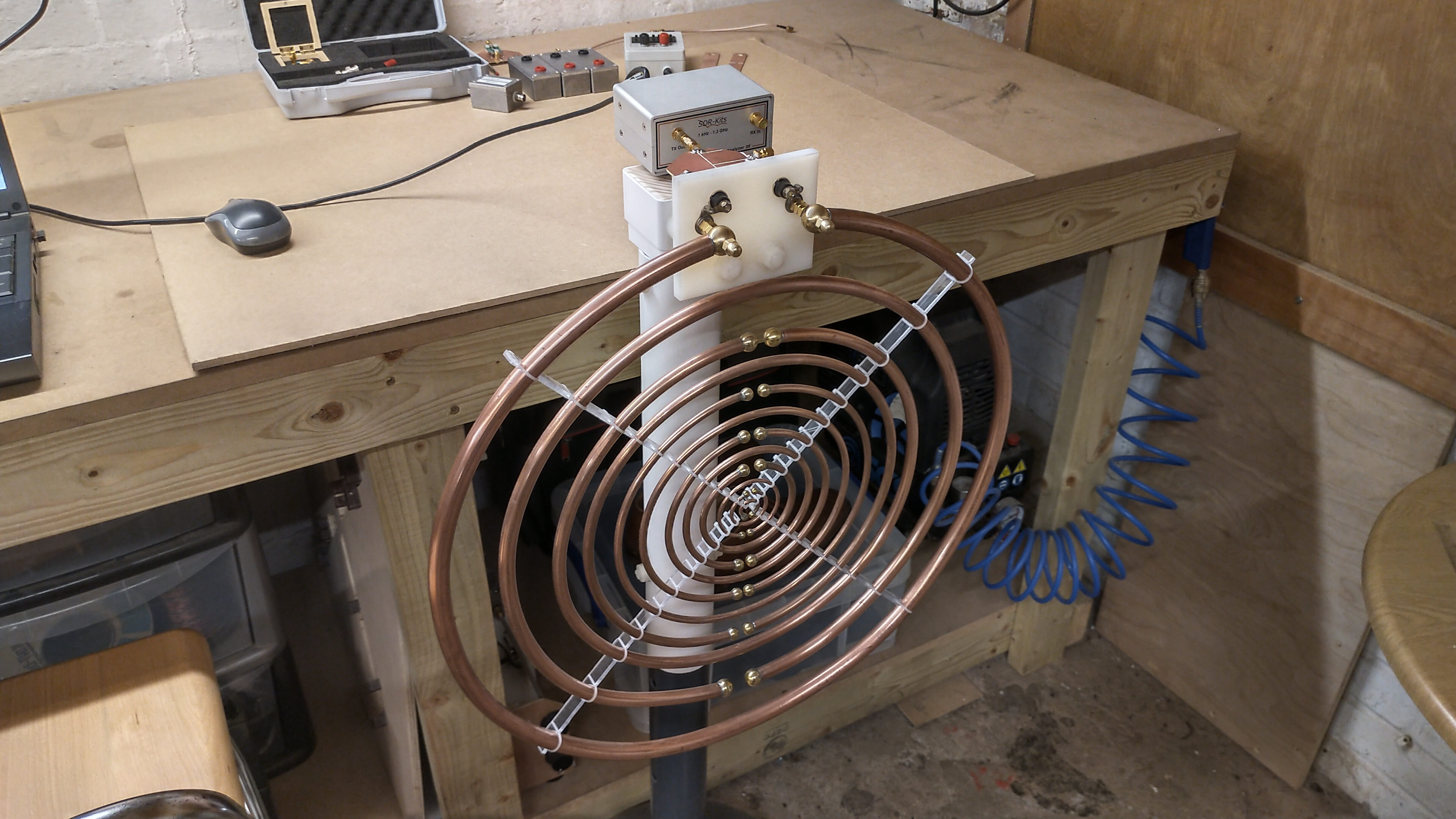

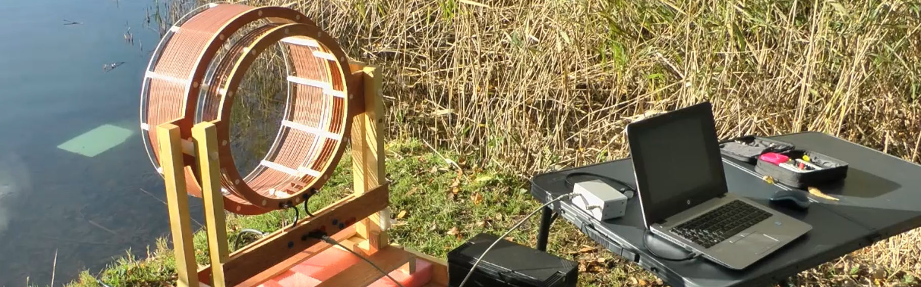
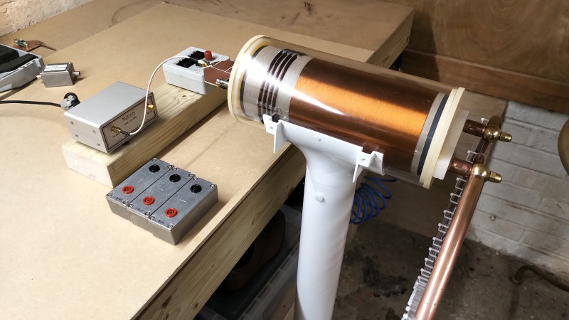
The original Lahkovsky Multiwave Oscillator (MWO) apparatus combines two Tesla style drive coils in a transmitter and receiver configuration, each consisting of a primary and secondary coil cylindrically mounted on axis. The top-load for both transmitter and receiver is a complex combination of concentric half-wave resonators. The impedance characteristics of even a single drive coil with top-load represents a complex measurement challenge with results that can span over a very wide frequency range, in the order of 100kc/s – > 1Gc/s.
In this first part the small signal impedance characteristics, Z11 (magnitude and phase) with frequency as seen by the generator, are measured for a single drive coil both with and without the MWO top-load over the lower frequency range of 100kc/s – 20Mc/s. In this measurement the impedance characteristics are dominated by the drive coil which will mask any higher frequency measurements pertaining to the MWO top-load. For this reason the top-load is measured individually in part 2 in the frequency range 100kc/s – 1.3Gc/s. Subsequent parts will look at the overall MWO system impedance characteristics when both transmitter and receiver are combined together in the original Lahkovsky arrangement, and later in an optimised and balanced drive arrangement as designed and presented by Dollard[1].
In this first part the following measurements are presented:
1. Z11 (magnitude and phase) with frequency for a drive coil without MWO top-load in the range 100kc/s – 20Mc/s
2. Z11 for the drive coil combined with MWO top-load, and over the same frequency band.
3. Primary tuning measurements to match the resonant frequency of the primary coil, (with series loaded Cp), to the secondary coil at the fundamental, second, and third harmonics.
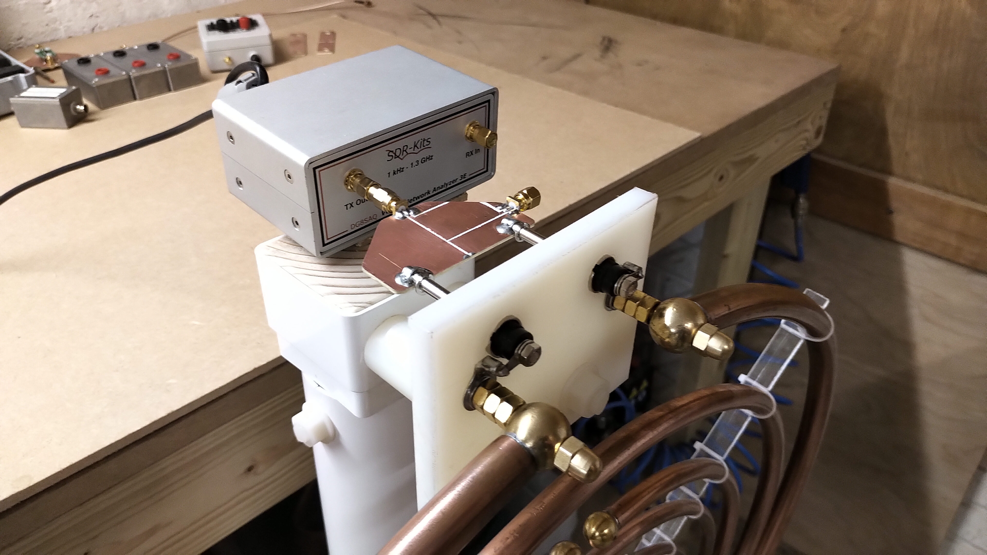
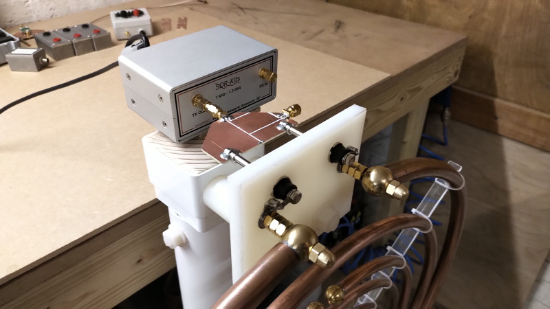
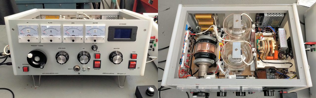
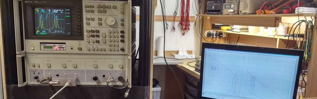
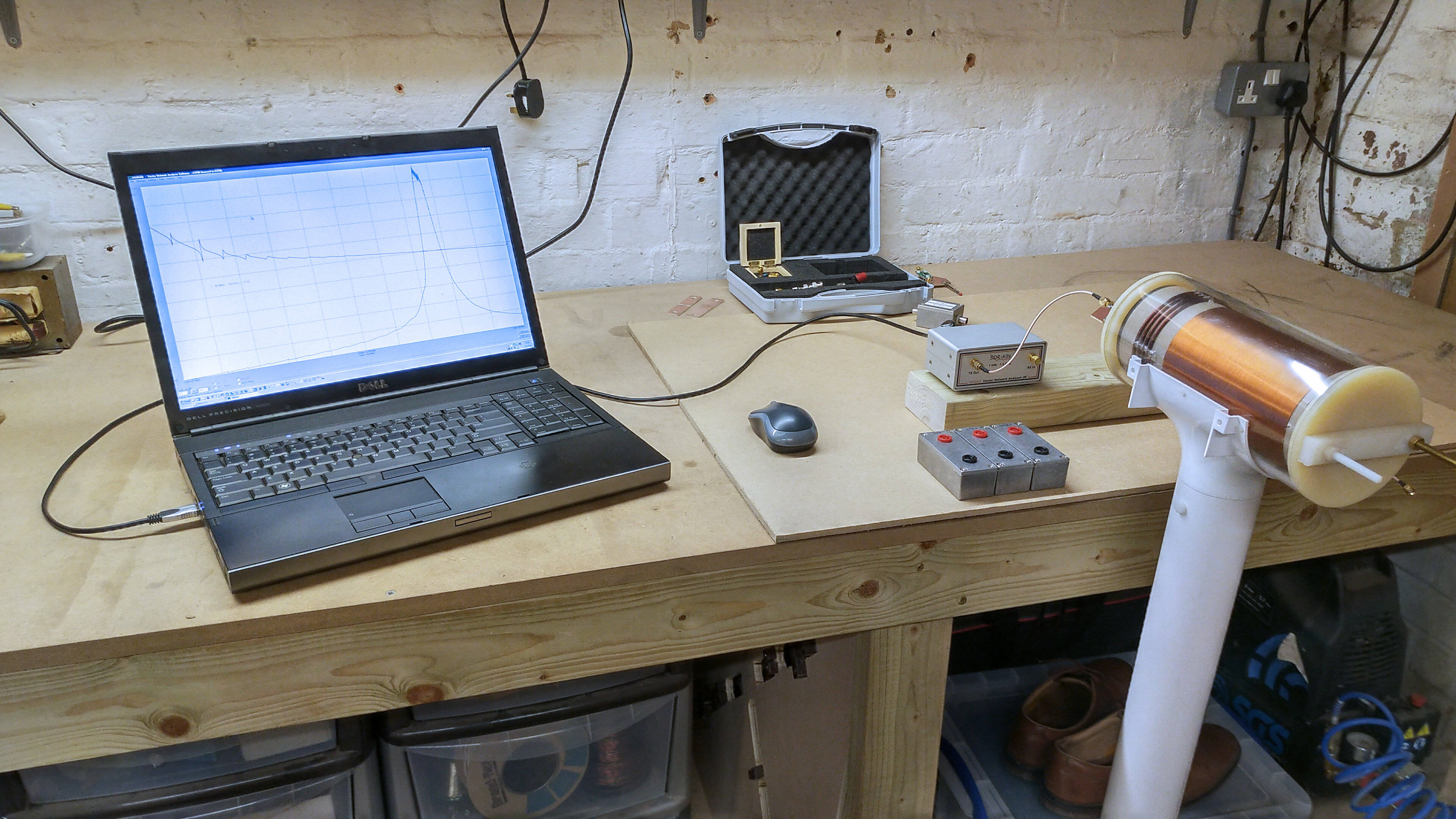
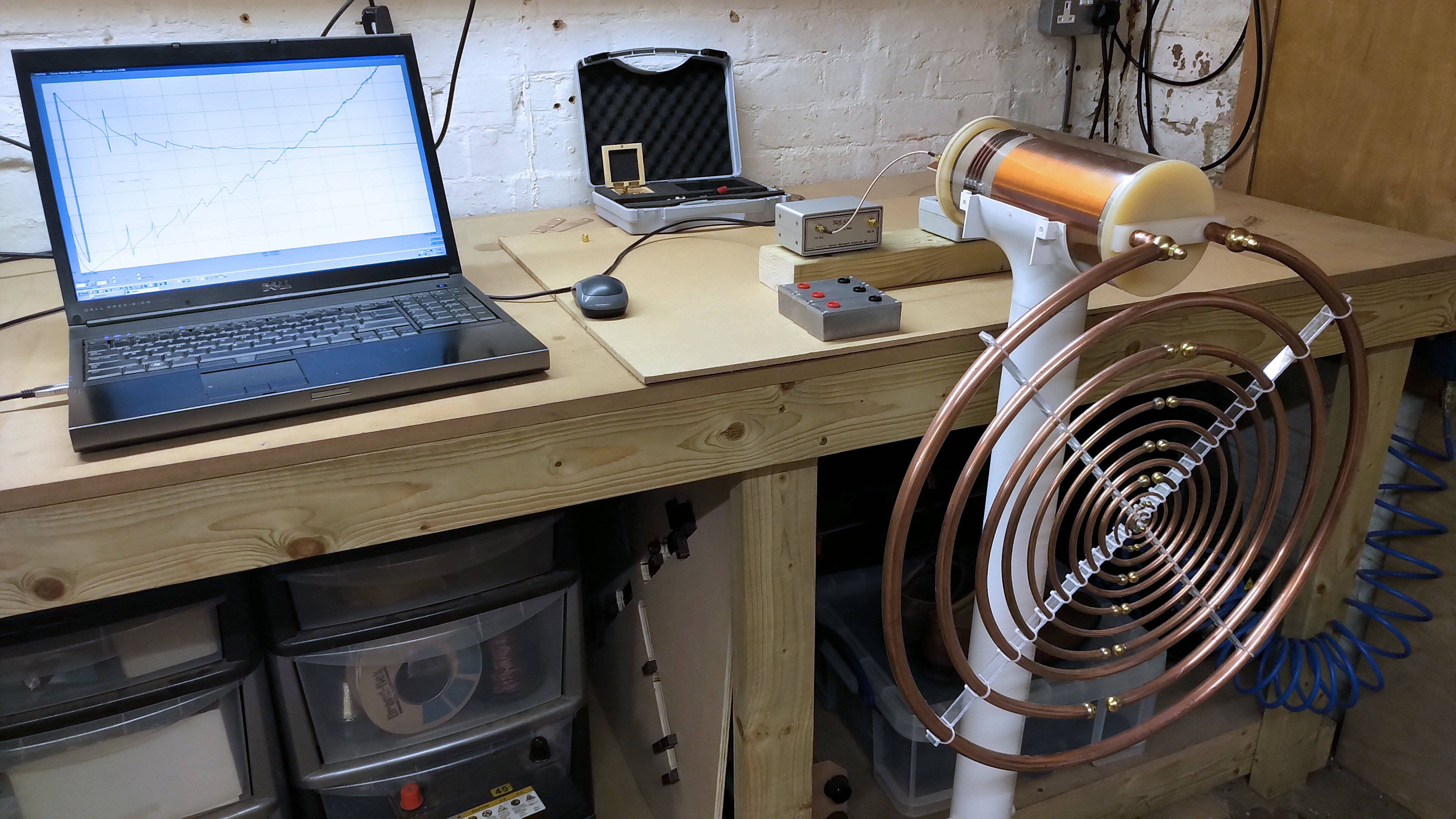
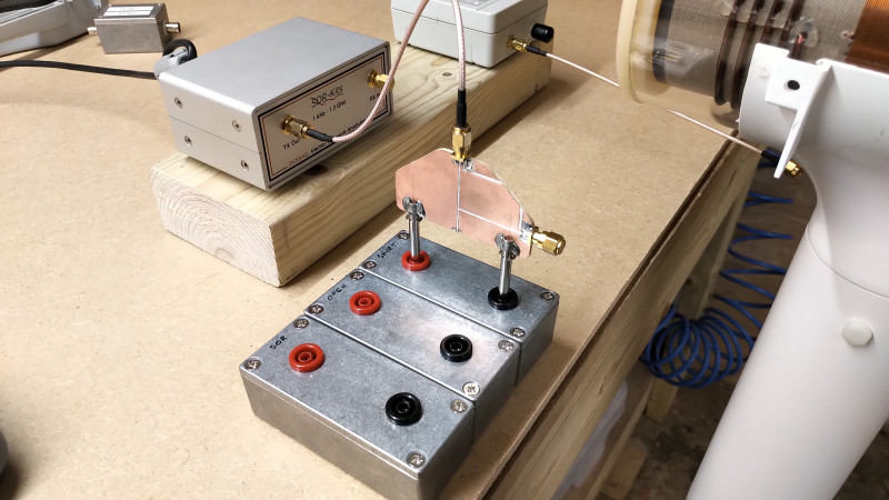
The SDR-Kits Vector Network Analyser 3E (VNA-SDR) was used to make all Z11 measurements, and the apparatus and method of measurement is shown in Figures 1 below.


To view the large images in a new window whilst reading the explanations click on the figure numbers below.
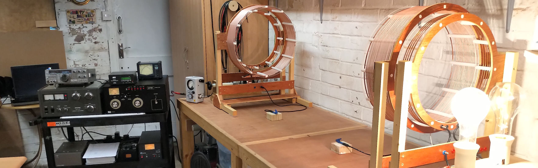
Fig 1.1. Shows the overall measurement setup with the VNA-SDR connected to the drive coil by a short SMA terminated RG316 cable, and the other end to the coil feed adapter, and standard calibration modules.
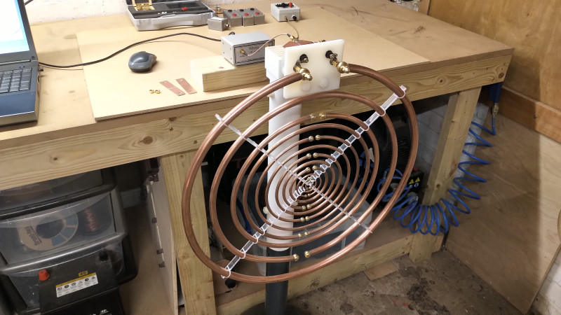
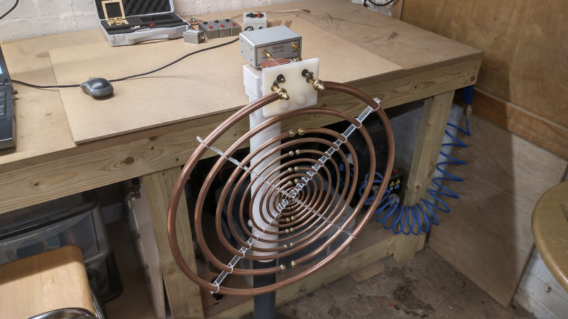
Fig 1.2. The drive coil used in these measurements has 4.5 primary turns of AWG 10 ~2.5mm diameter magnet wire, and the secondary has 248 turns of AWG 24 ~0.51mm diameter magnet wire. The top-end of the primary coil is connected directly to the bottom-end of the secondary coil and forms the negative or ground terminal. The positive or drive terminal is connected to the bottom-end of the primary coil, and the top-end of the secondary can be seen emerging from the coil through a brass bolt which attaches to the driven top-load. Both coils are wound anti-clockwise on the former from the base.
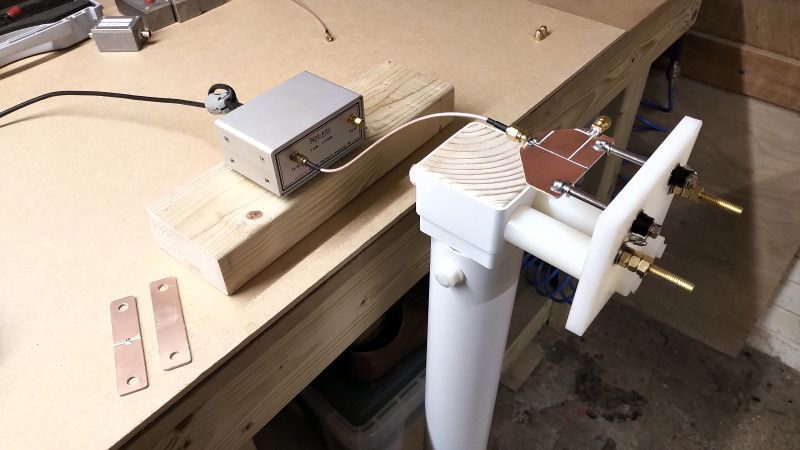
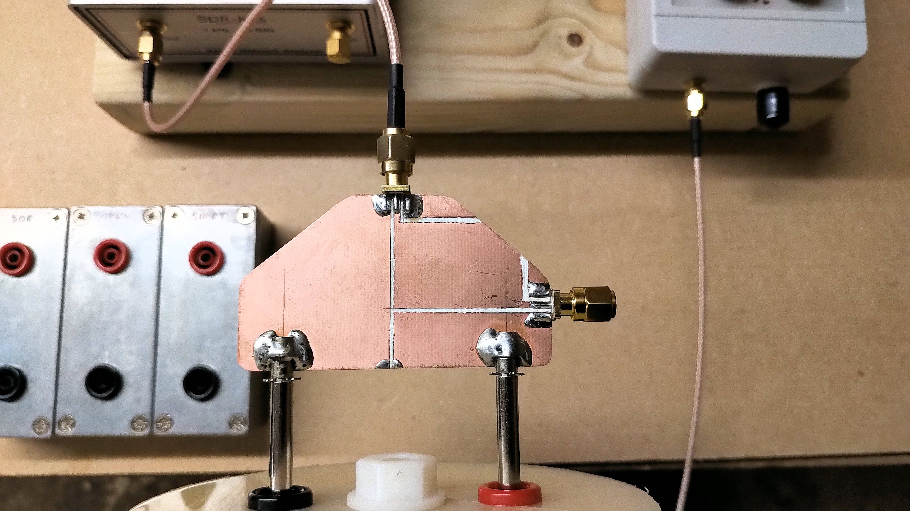
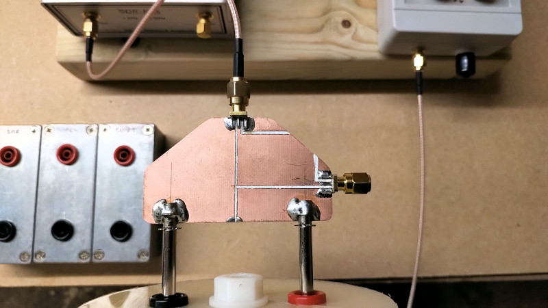
Fig 1.3. In order to make an accurate measurement of Z11 it is necessary to calibrate the VNA-SDR as close to the drive coil as possible. In this case the calibration plane is extended to the input of the primary coil terminals, (two 4mm high voltage shielded terminals), via a signal feed adapter pcb (SFA). The SFA can be removed from the drive coil by drawing the two-pronged 4mm probes out of the drive coil terminals. With the SFA disconnected the VNA-SDR can be calibrated by fitting an open, short and 50Ω standard load to the end of the SFA. The effective calibration plane then becomes the input to the drive coil, and spurious impedance effects due to any cables and the SFA itself can be removed from the final results. When calibrated, a frequency scan of the SFA with the 50Ω standard load will show a flat impedance line for |Z|, (magnitude of the impedance). The phase of this scan will swing repeatedly between ±180° indicating the near perfect match between the calibration plane and the 50Ω standard load.
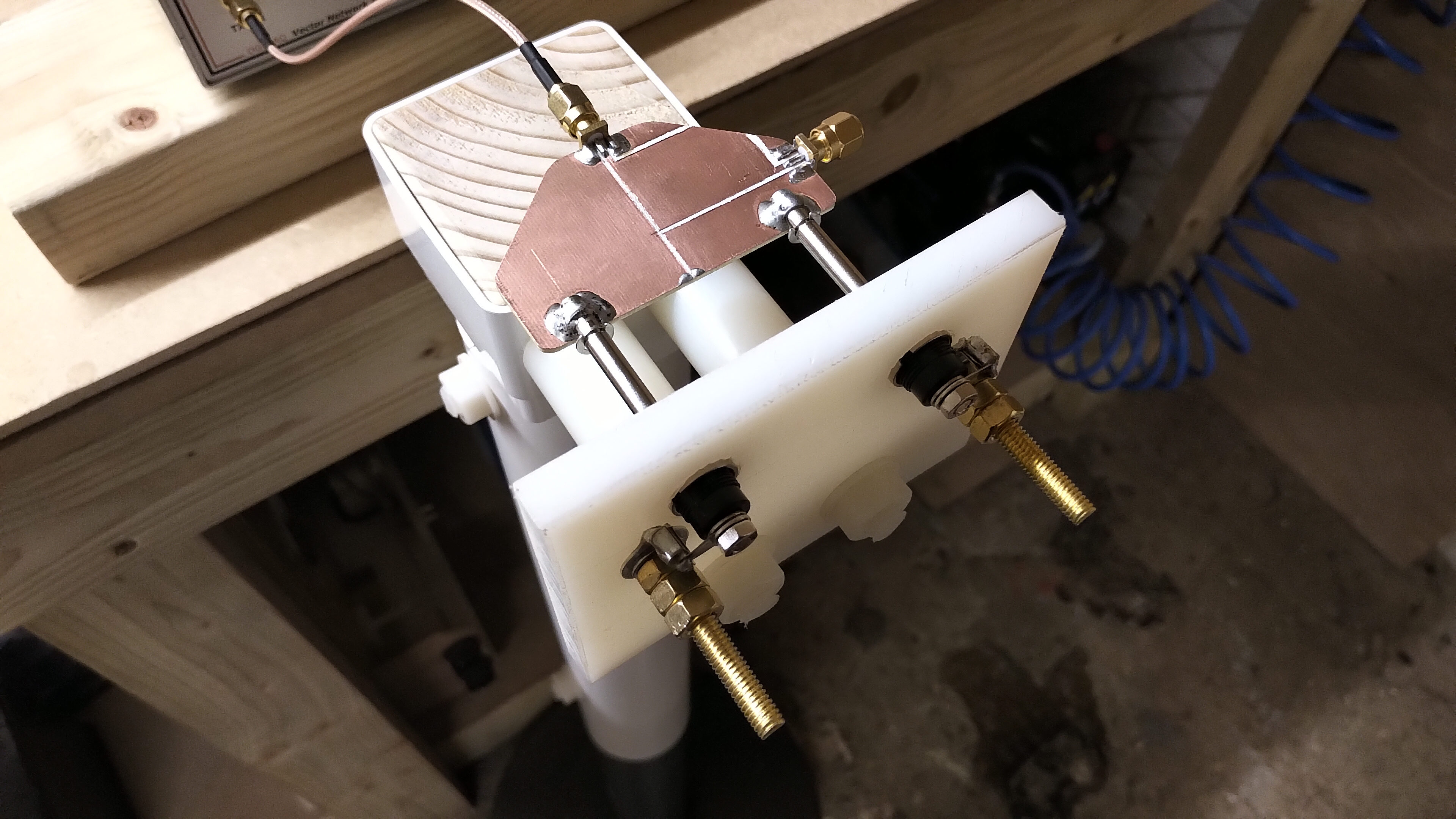
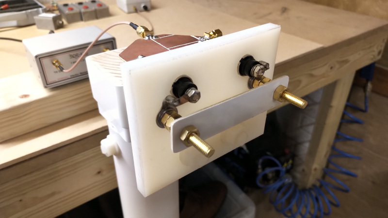
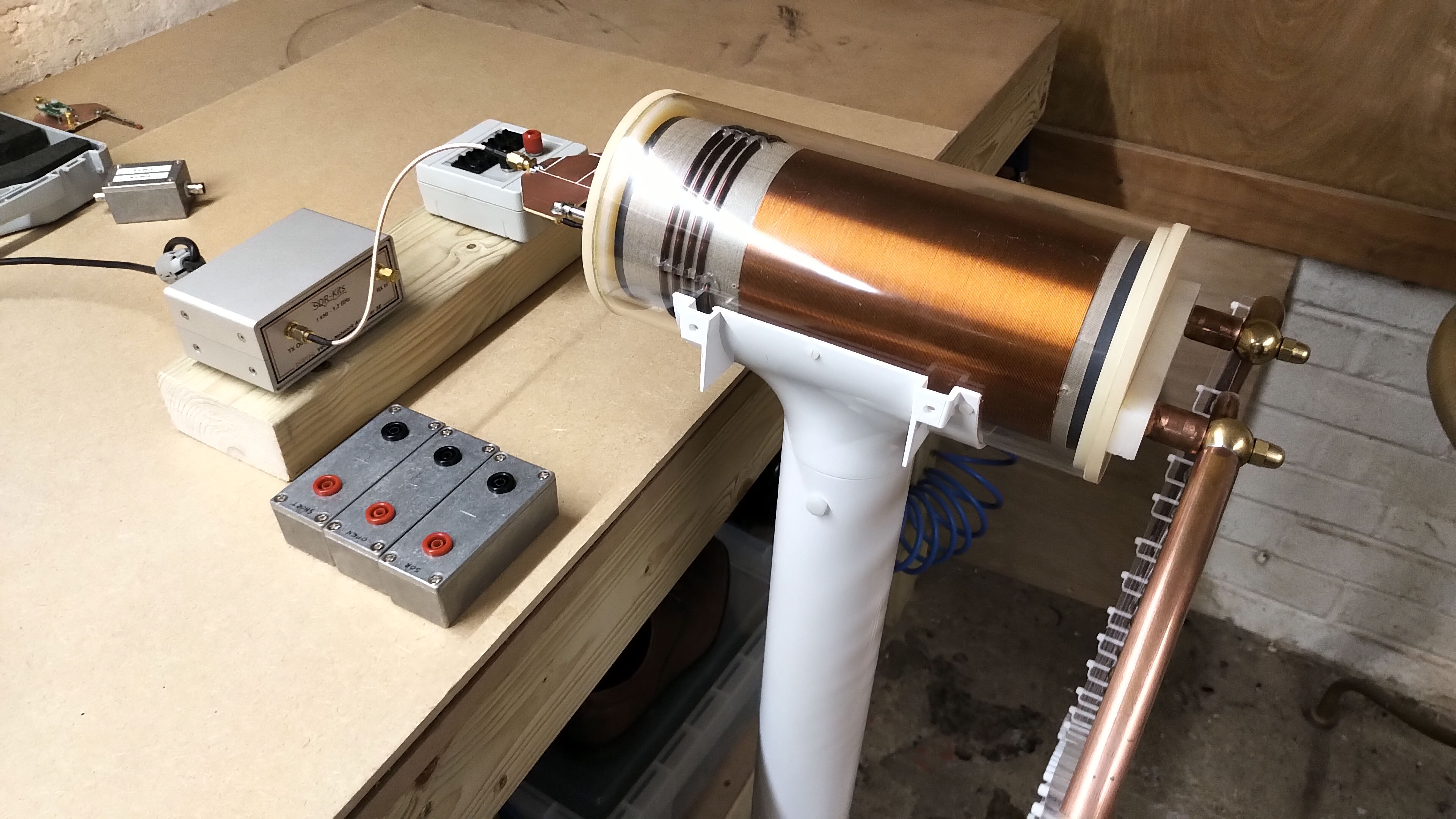
Fig 1.4. Shows a close-up of the SFA connected directly to the two high voltage drive terminals in the base of the drive coil. The SFA has an SMA input feed and is then connected via equal weights of copper to the series connection point. The black terminal indicates the negative or ground point where both primary and secondary are connected together, and the red terminal the high voltage feed end of the primary. The series connection point in the positive terminal allows for a calibrated capacitance box to be connected in the primary circuit for tuning measurements. In this picture the series connection is not being used and is terminated with a SMA short. In tuning measurements, when series capacitance CS is added, the SFA must first be calibrated with the capacitance box connected to the SFA with a nominal 1µF set at its output. The 1µF series capacitance has a very low impedance at the measurement band of interest and acts effectively as a short-circuit of the series connector during the calibration procedure. During tuning measurements the capacitance of the box is reduced in the range 100pF – ~ 50nF. The capacitance box itself uses surface mount standard capacitance values and can be reasonably used with SMA connection up to ~ 100Mc/s. The SFA is an unbalanced feed adapter and takes an unbalanced coaxial cable input directly to a balanced two terminal output without any compensation for this change in balance. A similar SFA was also tried which incorporated an RF (upto ~ 3Gc/s) balun in order to effect the transformation between the unbalanced and balanced connections. However, even with calibration the balun SFA proved to be less effective to measure Z11 accurately and cleanly, as it dominated the impedance changes in the frequency band masking changes due to the drive coil further downstream. The standard SFA was therefore used with careful calibration up to the intended reference plane at the input terminals to the coil.
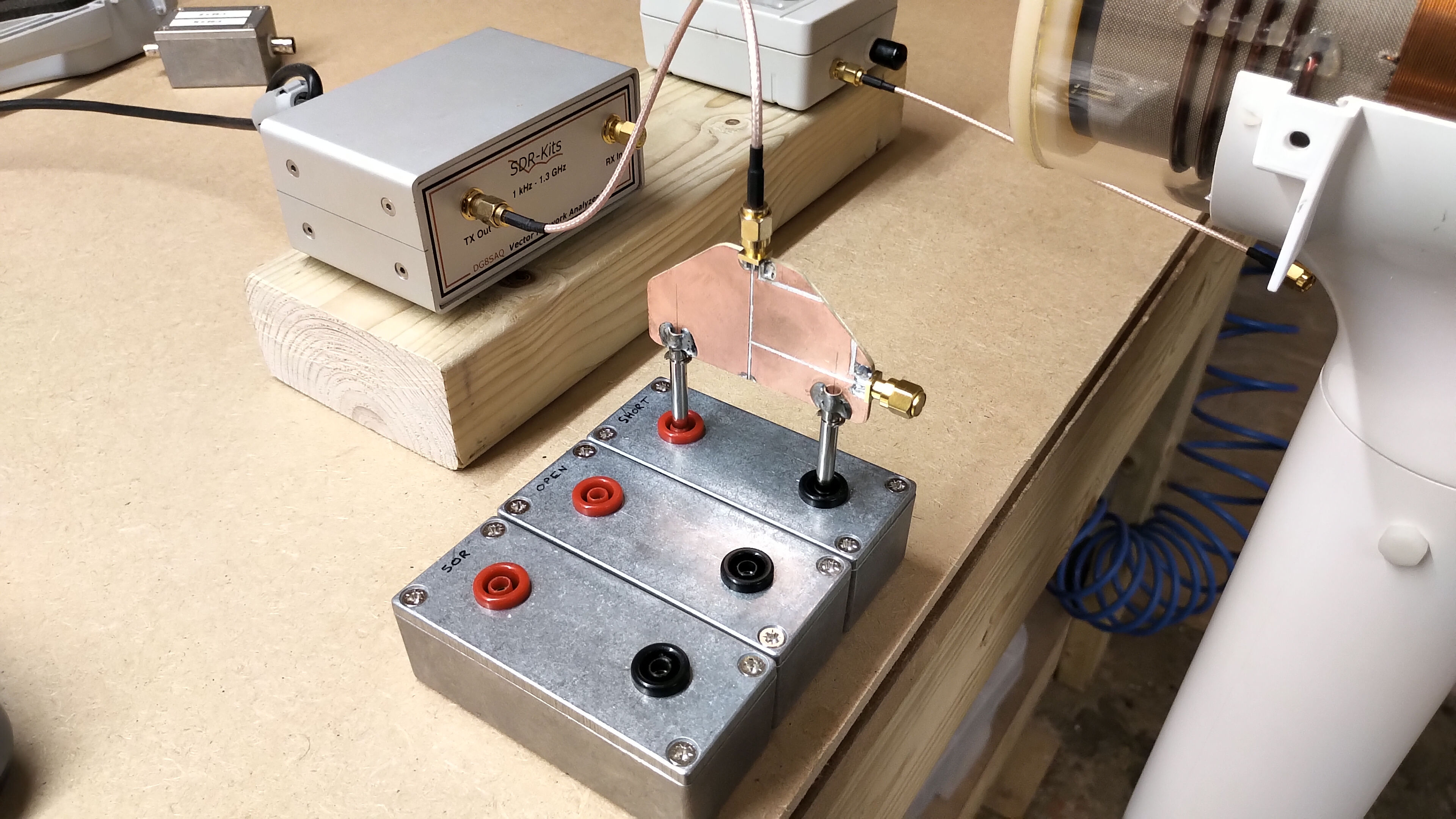
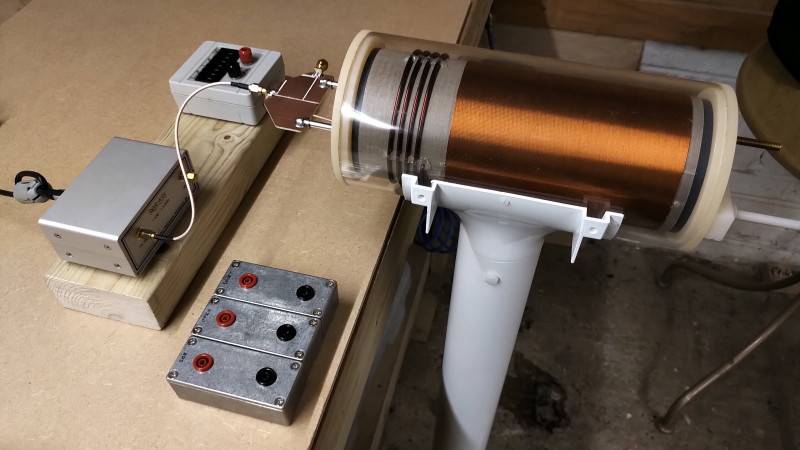
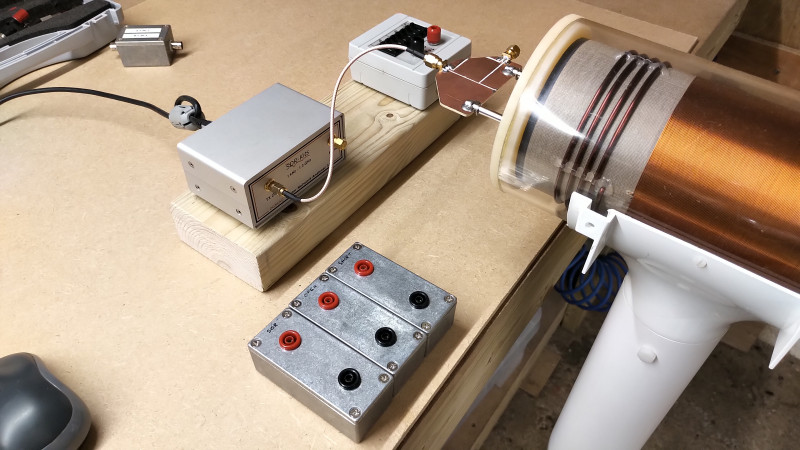
Fig 1.5. Shows the calibration procedure where the SFA is connected in turn to the standard calibration modules, here connected to the short circuit module. In this case the series capacitance terminal is not being used and is shunted with an SMA short.
Fig 1.6. Shows the SFA in measurement configuration and after calibration, where a 1nF series capacitance is added to the primary feed. The calibrated capacitance box can be adjusted in 1pF increments in the range ~30.5pF – ~10µF, where the parasitic capacitance of the box with SMA cable and when set to zero is ~30.5pF.
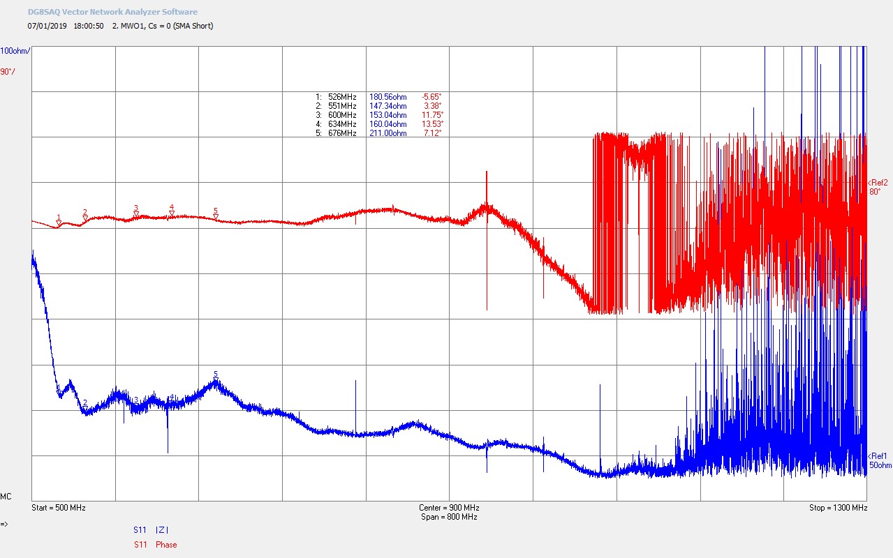
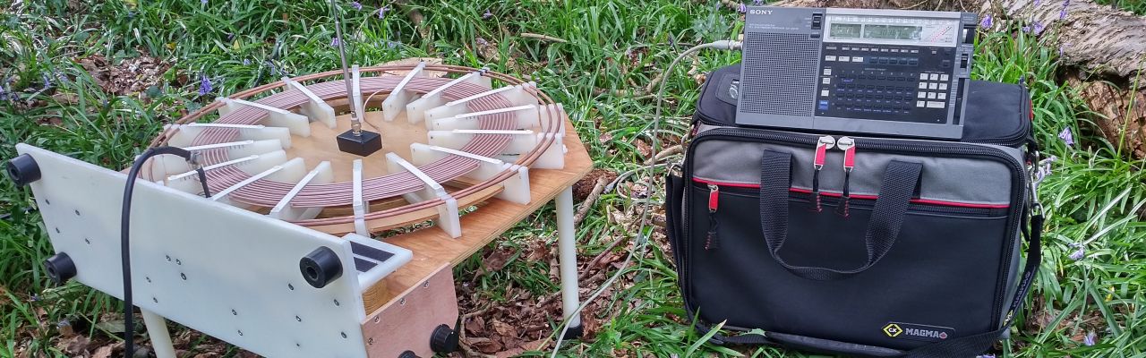
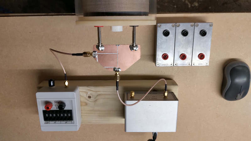
Fig 1.7. Shows the overall measurement setup with the top-load connected, and then calibrated and measured in the same procedure as previously discussed. The outer ring of the top-load forms an effective wire extension and capacitive load to the top of the secondary coil, which will both reduce considerably the fundamental resonant frequency and Q-factor of the drive coil. When compared with the drive coil without top-load the outer ring forms a λ/4 driven ring, which is coupling to 11 other λ/2 resonating rings. Given the size of the outer driven ring, and the proximity of the inner rings the coupling factor is considered to be quite high between the driven ring and the inner resonators, which will tend to constrain the free resonation of the inner rings and considerably quench the Q and hence measurements at much higher frequency. This is considered more closely in part 2.
Fig 1.8. Shows in more detail the mounting points at the top-end of the secondary and the MWO top-load.
Figures 2 below show the Z11 impedance characteristics of the calibrated reference plane, the drive coil, and primary and secondary tuning with series added capacitance, of the drive coil only.

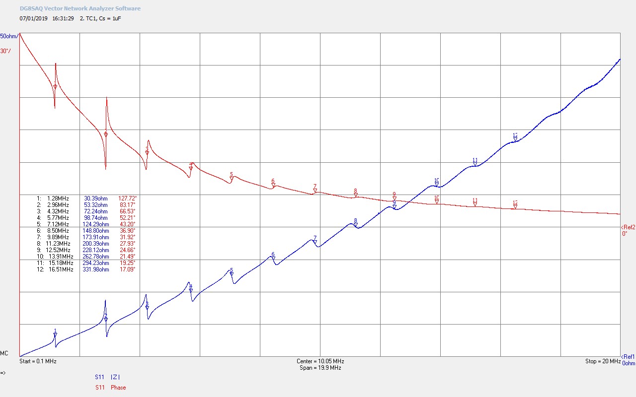
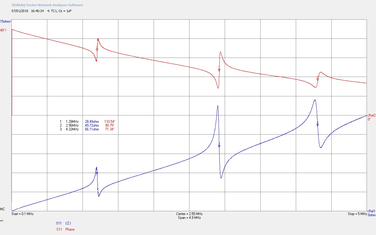
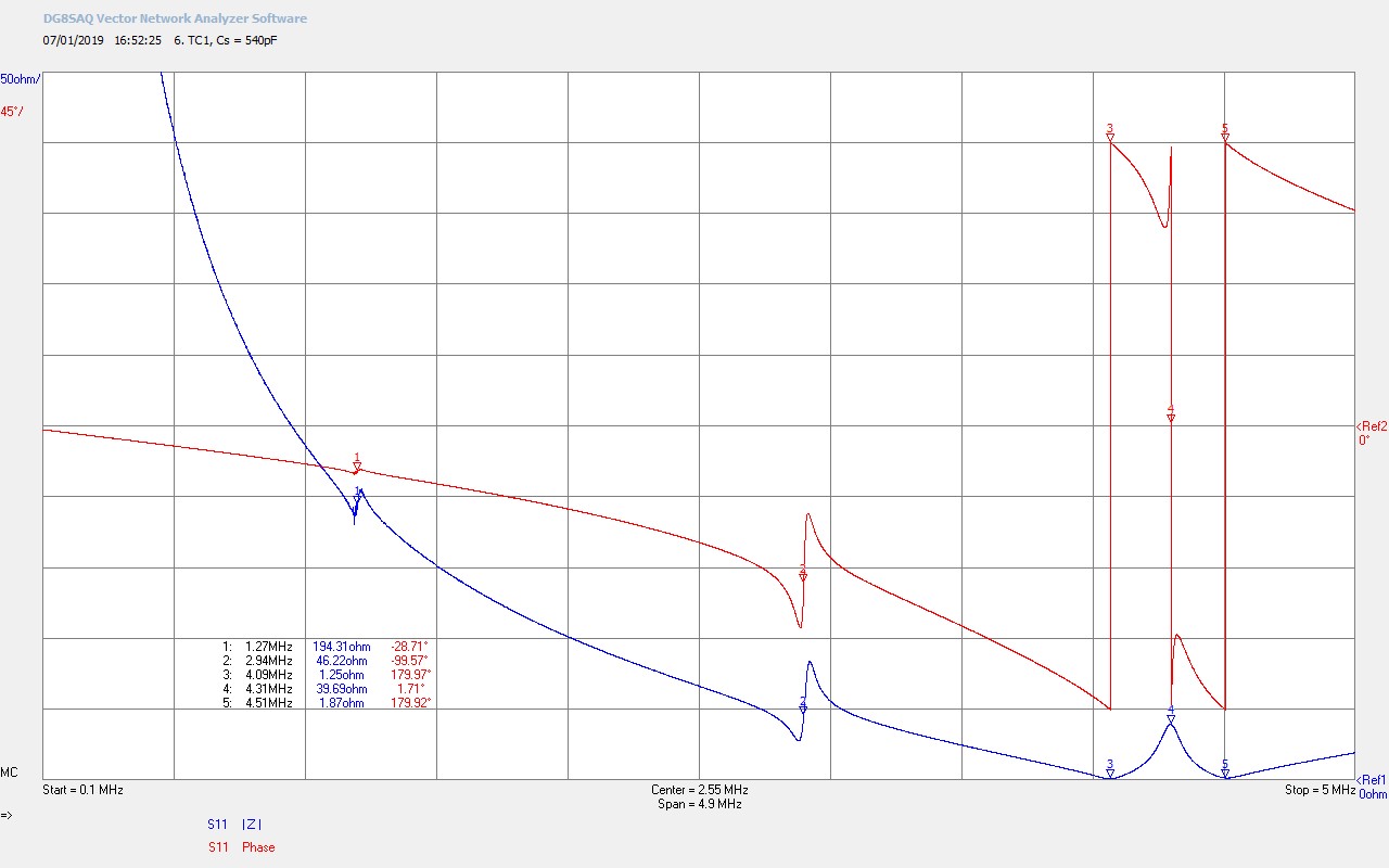

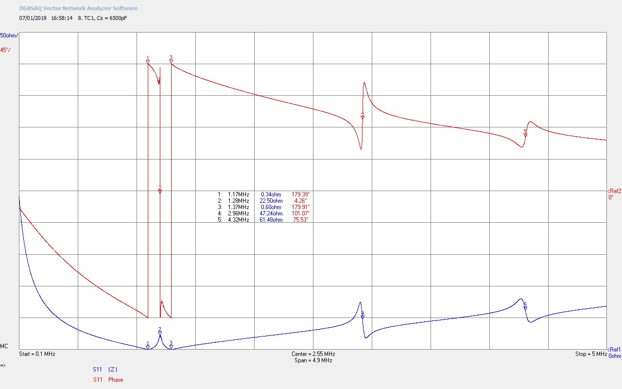
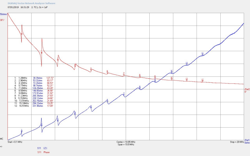
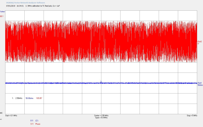
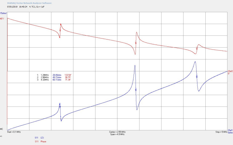
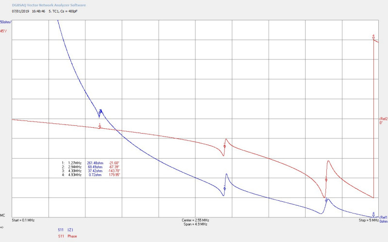
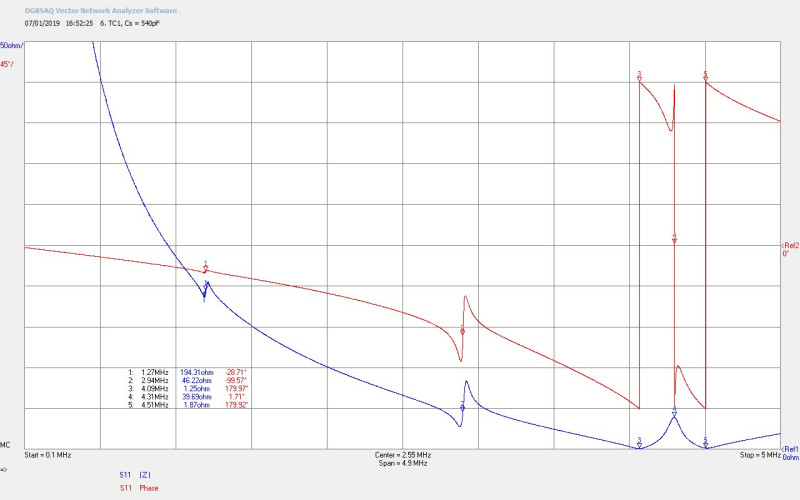
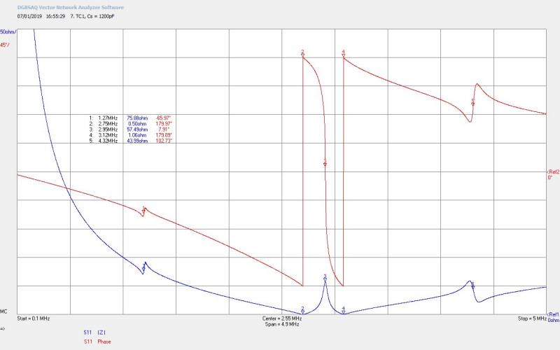
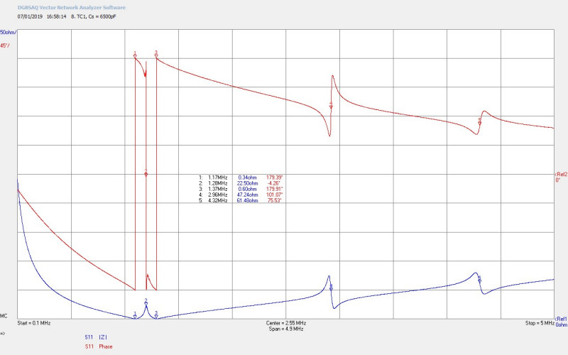
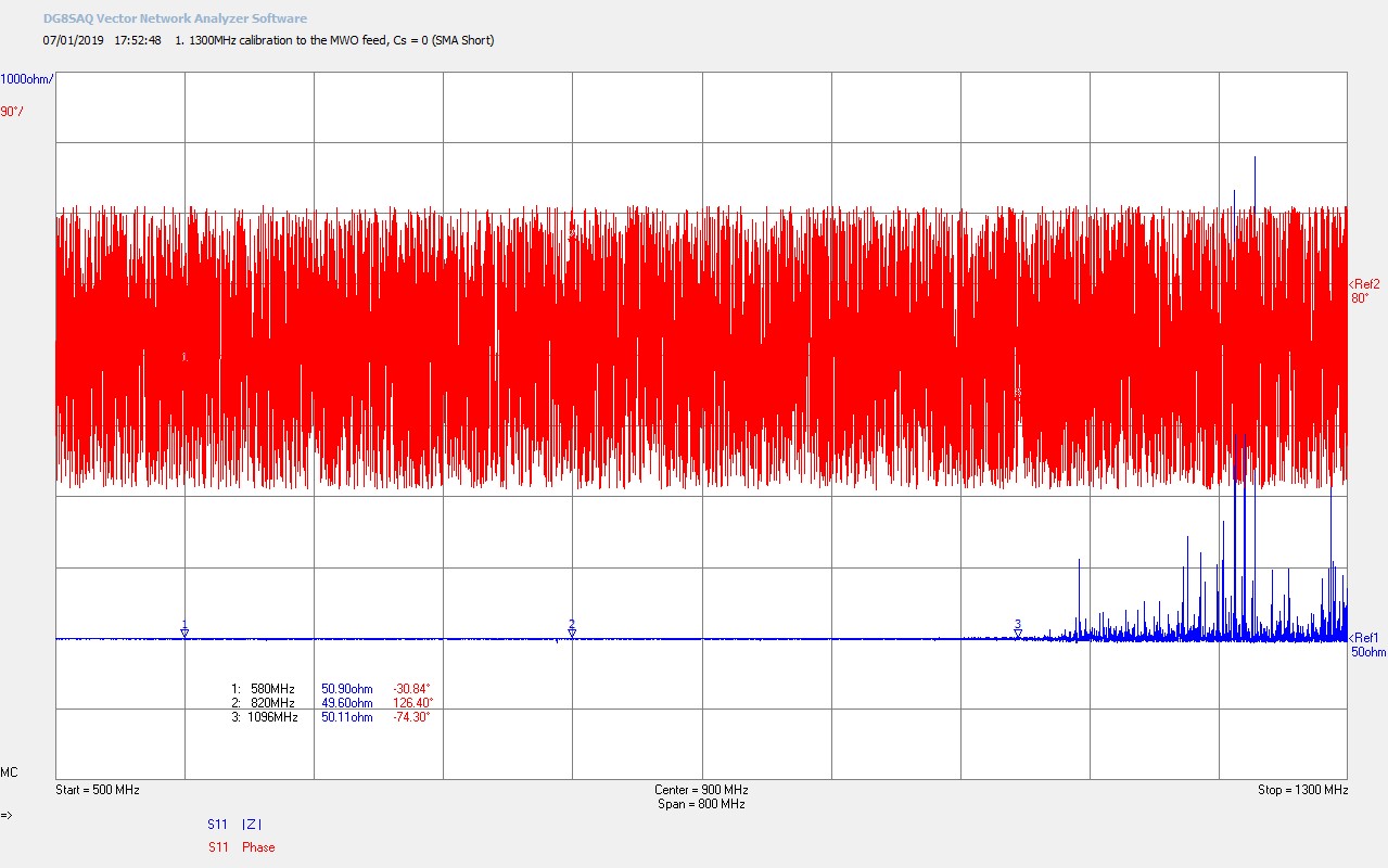
Fig 2.1. Shows the calibrated reference plane of the SFA when connected to the 50Ω standard load over the wideband range 100kc/s – 20Mc/s. The calibration is as expected and accurate over the band, with a slight phase variation between ~ 3 – 3.5Mc/s indicating a resonance in the signal path between the calibration plane and the VNA-SDR which has been normalised out by the calibration procedure.
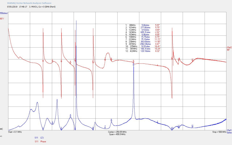
Fig 2.2. The impedance characteristics of the drive coil with the series capacitance Cs = 1µF, showing a wealth of resonant peaks and corresponding phase changes from the fundamental resonant frequency FS of the secondary coil at 1.28Mc/s up to the 12th harmonic FS12 (M12) at 16.51Mc/s. It is interesting to note that the 2nd harmonic FS2 at M2 is a stronger resonance than that of the fundamental at M1. This is further demonstrated in subsequent impedance results. The VNA-SDR allows for only 12 concurrent markers which is why the final two harmonics on the results are not marked. At frequencies above 20Mc/s the rapidly increasing inductive impedance of the primary masks out any further harmonic points of interest, and the impedance curve rises rapidly until the primary coil becomes self-resonant at ~38Mc/s.
Fig 2.3. Shows the calibrated reference plane of the SFA when connected to the 50Ω standard load over the narrowband range 100kc/s – 5Mc/s. With more accurate calibration in the narrowband it can be noted that the phase variation seen in Fig. 2.1 has now been completely normalised out of the reference plane.
Fig 2.4. Shows the narrowband impedance characteristics for the fundamental FS and the first two harmonics FS2 and FS3. Here the difference in magnitude of the resonance between FS and FS2 can be very clearly observed, although the Q of the coil remains very similar for both frequency points. The magnitude of the impedance |Z11| ~ 28.5Ω at FS, and ~ 49.7Ω at FS2 would significantly impede currents developed in the primary from the generator, coupling very little power to the secondary and ultimately to the MWO top-load. The primary circuit will need to be brought into resonance with the secondary at the corresponding frequency in order to considerably reduce the driving impedance seen by the generator, and hence maximise the primary currents, and the amount of power transferred from the generator through the drive coils to the top-load. On the very far left of the scan at 100kc/s the 180° phase change FØ180 of the primary in resonance with the series capacitance CS can just be observed. This will be adjusted by varying CS in subsequent results in order to tune the primary resonant frequency to that of the secondary. Given the difference in magnitude between the fundamental at FS and the 2nd harmonic at FS2 it may be more optimal to arrange the primary to resonate at FS2 rather than the fundamental for normal experimental operation. This will be tested during experiments and reported in subsequent parts.
Fig 2.5. Here the series capacitance CS has been reduced from 1µF to 400pF which has increased FØ180 (the resonant frequency of the primary to M4 at 4.93Mc/s. At this point the impedance seen by the generator has reduced drastically to ~0.72Ω allowing for much larger primary currents. In this case FØ180 does not correspond to a resonant frequency in the secondary so reduced power would be transferred between the two coils. At lower frequencies in the measurement band, the impedance of CS is higher and has the effect of attenuating currents in the primary reducing considerably the magnitude of the lower resonant points, in this case considerably suppressing the fundamental resonance at FS. This scan clearly shows the effect of including a series resistance in the primary and making it resonant within the measurement band of interest.
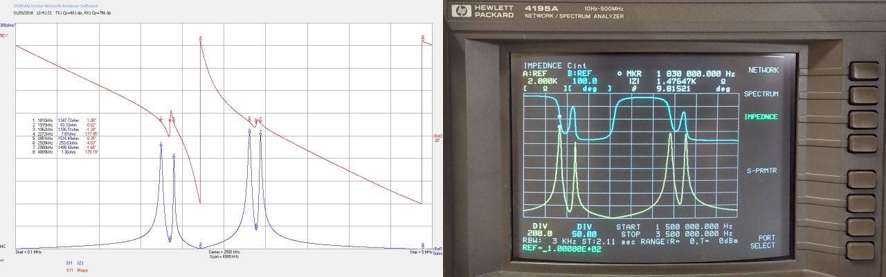
Fig 2.6. Here CS has been increased to 540pF which has brought the resonant frequency of the primary equal to the 3rd harmonic resonance of the secondary at M4 at 4.31Mc/s. As always with coupled resonant circuits, mixing of the signals causes beat frequencies and hence frequency splitting into two sideband frequencies where the impedance minimum points are at both the lower and upper resonant frequencies FL3 (M3) and FU3 (M5) respectively. If driven by a generator with CS = 540pF FL3 would be the best driving point since proximity coupling to the secondary top-load, or discharge of stored energy on the top-load, would momentarily increase the loading on the coil reducing slightly its secondary harmonic frequency towards FL3, and hence maximising transference of electric power between the primary and secondary coils.
Fig 2.7. Shows CS increased further to 1200pF which now tunes the primary resonance to the 2nd harmonic FS2 at M3 a frequency of 2.95Mc/s. Again frequency splitting occurs and the impedance of FL2 and FU2 are very low ~0.5 – 1Ω facilitating high current drive from the generator.
Fig 2.8. Shows CS finally increased to 6500pF which tunes the primary to the fundamental resonant frequency of the secondary FS at M2 at 1.28Mc/s. At FL (M1) the lowest impedance drive point is obtained of just 0.34Ω at 1.17Mc/s. Given the very similar minimum |Z| characteristics of both FS and FS2, when tuned respectively to the primary with corresponding values of CS, either the fundamental or 2nd harmonic could be used to operate the coil in experiments to explore MWO operation and effects.
Figures 3 below show the Z11 impedance characteristics of the calibrated reference plane, the drive coil, and the primary and secondary tuning with series added capacitance, of the drive coil with the MWO top-load.
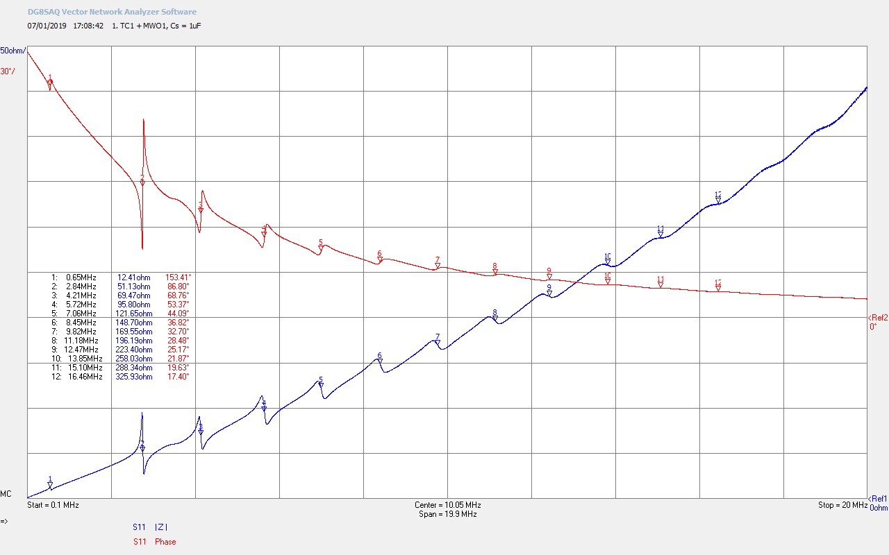
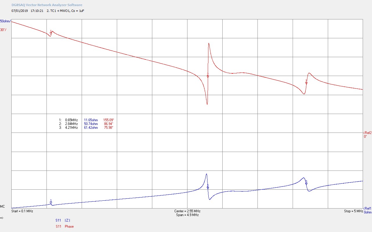
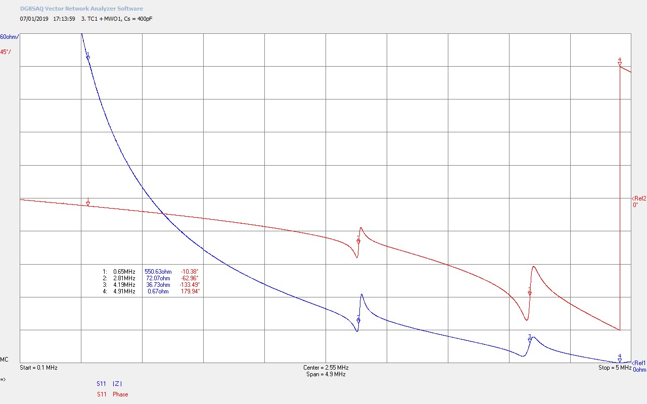
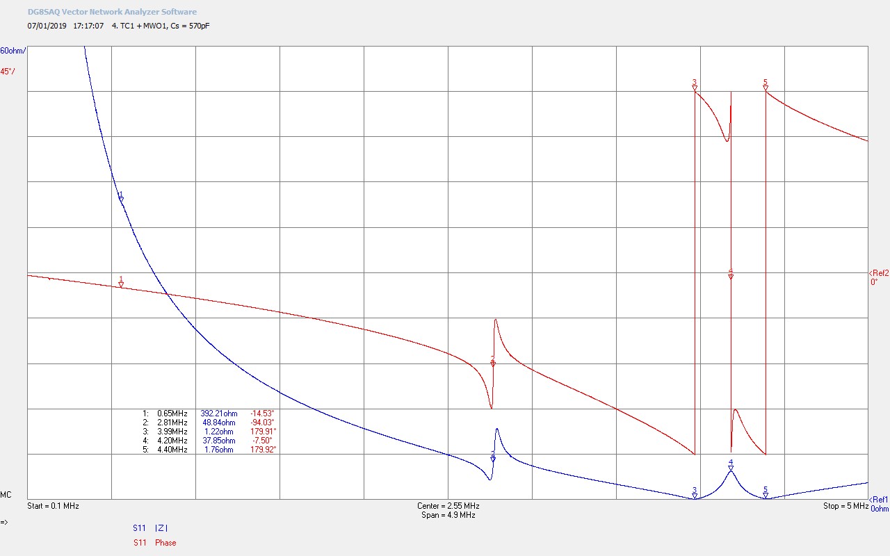
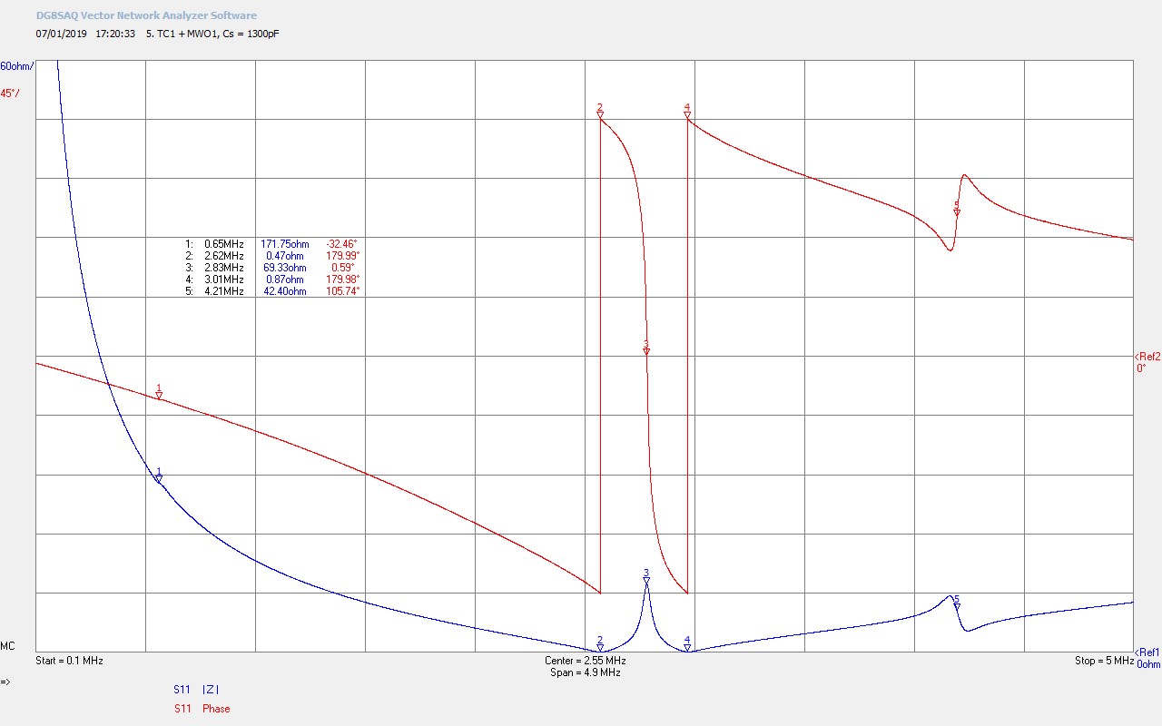
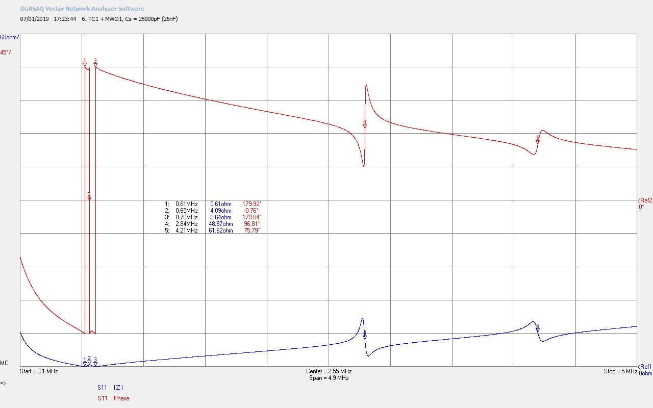
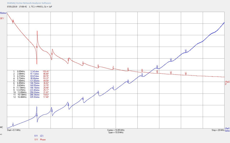
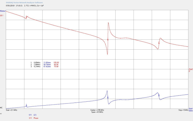
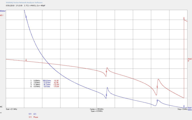
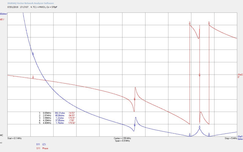
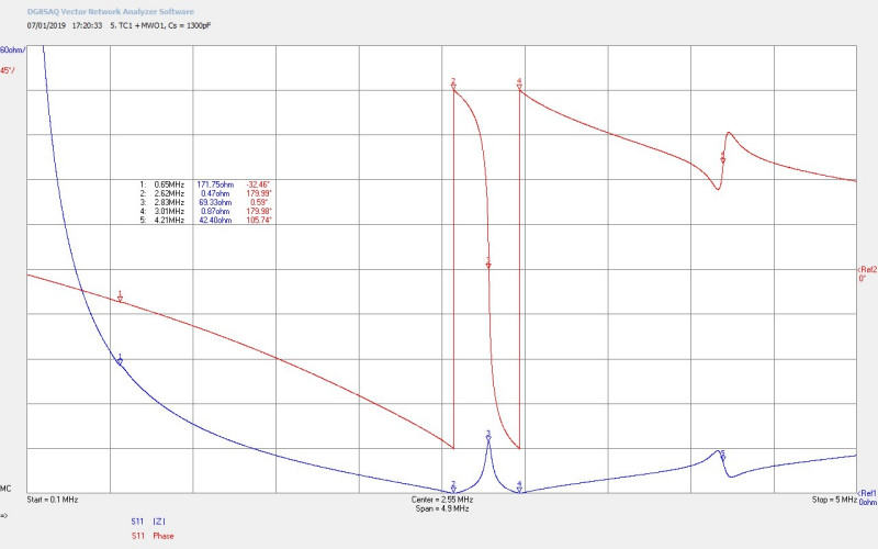

Fig 3.1. Shows the wideband scan for the drive coil with MWO top-load on the same horizontal and vertical scaling as in Figures 2. The top-load at lower frequencies represents a considerable capacitive load at the top of the coil, very similar capacitively to a toroidal, cylindrical, spherical, or sheet metal top-load added to a conventional Tesla coil apparatus. The frequency of this scan is too low to show any of the high frequency features that result from the resonant rings of the MWO, (see part 2 for these features), but the capacitive loading of the MWO top-load could be clearly seen in this lower frequency scan. The biggest effect is noted at M1 at FS1 the fundamental resonance of the secondary which has reduced from 1.28Mc/s to 650kc/s, a 49.2% reduction . The 2nd and 3rd harmonics at FS2 and FS3 respectively have also reduced but in a much smaller range than the fundamental. FS2 has reduced from 2.96Mc/s to 2.84Mc/s a 4.1% reduction, and FS3 from 4.32Mc/s to 4.21Mc/s a 2.5% reduction. Higher harmonics also reduce with progressively reducing amounts up to FS12 at M12 which reduces from 16.51Mc/s to 16.46Mc/s a 0.3% reduction. It can be seen for this arrangement of drive coil the fundamental resonant frequency would be very sensitive and easily effected by metal loading to the top end of the secondary, the close proximity of metallic structures, or even to the proximity of partially conducting mediums such as the human body.
Fig 3.2. The narrowband scan shows the large change in the fundamental in relation to the 2nd harmonic both in frequency shift and in the magnitude of the impedance and phase change. The MWO top-load has considerably quenched the fundamental of the drive coil, whilst leaving the 2nd harmonic very similar to the coil only results (Figures 2) both in frequency and the magnitude of the impedance and phase.
Fig 3.3. Series capacitance CS = 400pF as before shows the primary resonance in the band, but in this case has completely quenched the already weak fundamental resonance. It can be seen that driving the MWO at the 2nd harmonic during experiments and operation may lead to considerably more stable and reliable system characteristics.
Fig 3.4. Shows the primary tuned at FS3 at M4 at 4.20Mc/s and a slightly increased series capacitance required to tune, increased from 540pF to 570pF.
Fig 3.5. Shows the primary tuned at FS2 at M3 at 2.83Mc/s and again a slightly increased series capacitance required to tune, increased from 1200pF to 1300pF. It can be noted that the fundamental resonance FS can now just be discerned at M1 at 650kc/s.
Fig 3.6. Shows the primary tuned at FS at M2 at 0.65Mc/s with FL = 610kc/s and FU = 700kc/s. The primary is tuned when CS = 26000pF (26nF) which is a very large increase on the 6500pF required without the MWO top-load. At FL (M1) the impedance seen by the generator in the primary is now 0.61Ω which is no-longer the lowest driving impedance. With CS = 1300pF and tuned to FS2 the driving impedance at FL2 is 0.47Ω which indicates that better power transfer from the generator to the secondary could be effected by driving the MWO at the 2nd harmonic. At this point the system would also be more stable and less effected by proximity of metal structures and other partially conductive mediums including the human body.
The lower frequency impedance measurements have shown a wealth of frequency harmonics associated with the Tesla style drive coil, and can be tuned progressively with the primary of the drive coil via series capacitance to make use of the system at different designed resonant frequency points. The MWO top-load at lower frequencies introduces a considerable capacitive load on the drive coil which has a large quenching effect on the fundamental resonant frequency of the system, and suggests a shift of optimal setup away from being driven at the fundamental and towards the 2nd harmonic where greater transference of electric power should be possible, and the system would be more stable and tolerant of loading conditions on the drive coils, the MWO top-load directly, and also from proximity of other conducting and partially conducting mediums. It will be interesting to determine if this changes when both the transmitter and receiver are combined in the full Lahkovsky MWO system, and also whether these effects can be directly demonstrated through experiments in the operation of the complete MWO system.
Click here to continue to part 2 of the multiwave oscillator impedance measurements.
1. Dollard, E., Design and presentation of an optimised and balanced MWO power supply and drive coils., Energy, Science, and Technology Conference (ESTC), 2018.
2. Vril Science, Lahkovsky Multiwave Oscillator, 2019, Vril