Multiwave Oscillator Impedance – Part 2

In part 2 of the multiwave oscillator impedance (MWO) measurements we take a look at the high frequency impedance characteristics Z11 for the MWO resonator rings (top-load). The MWO Tesla style drive coil measured in part 1 needs to be separated from the MWO top-load for this type of measurement, because the impedance and load of the drive coil masks out any resonant features at higher frequencies, making it impossible to measure the MWO when connected to the top of the secondary coil and measured at the input to the primary coil.

Experiments, operation, and measurements in Tesla coil based systems, and indeed in my own research regarding the displacement and transference of electric power, are normally limited to experimental apparatus which operates at maximum in the HF band < 30Mc/s of the electromagnetic spectrum. At 30Mc/s the corresponding wavelength λ is 10m. As a standard rule of thumb in high frequency or RF measurements the feature size of the element under measurement should be < λ/10 to be considered as a discrete lumped element in the system, and therefore not subject to impedance transformations through transmission line characteristics or other distributed network characteristics. At the upper end of the HF band this means that active measurement regions < 1m in size or length can be considered to have only small, if any, transformation and change on the impedance outside of that attributed with its discrete lumped element network.

As we progress to higher frequency measurements in the VHF band (30 – 300Mc/s) and even above in the UHF band (300Mc/s – 3Gc/s) very great care needs to be taken regarding the length and size of cabling and connections, the feature sizes of components within the measurement network, the impedance match or mismatch between transmission line sections and discrete components, and any other stray, parasitic, or proximity effects arising from boundary conditions that are both metallic or dielectric in nature. Accordingly, much greater care and attention needs to be taken to calibrate as accurately as possible directly to the plane of measurement, and then to normalise out measurement effects between the calibration plane and measurement apparatus.

In this part we are concerned with measurement up to ~1Gc/s (λ = 30cm), and where the λ/10 length is only 3cm. At λ/4 quarter-wavelength we would expect to see a complete impedance transformation along a transmission line from a very low impedance (short-circuit) at the output of the source generator to a very high impedance (open-circuit) at the end of a wire or measurement plane. Accordingly we need to keep connections small and efficient which represents in itself a unique challenge when connecting to the MWO rings, which at UHF frequencies represent a large distributed network of inter-connected transmission line elements, with complex boundary conditions. Subsequent parts will look at the MWO rings as an antenna with corresponding radiation resistance and defined radiation pattern and particularly in relation to the transmitter – receiver configuration of the complete MWO system.

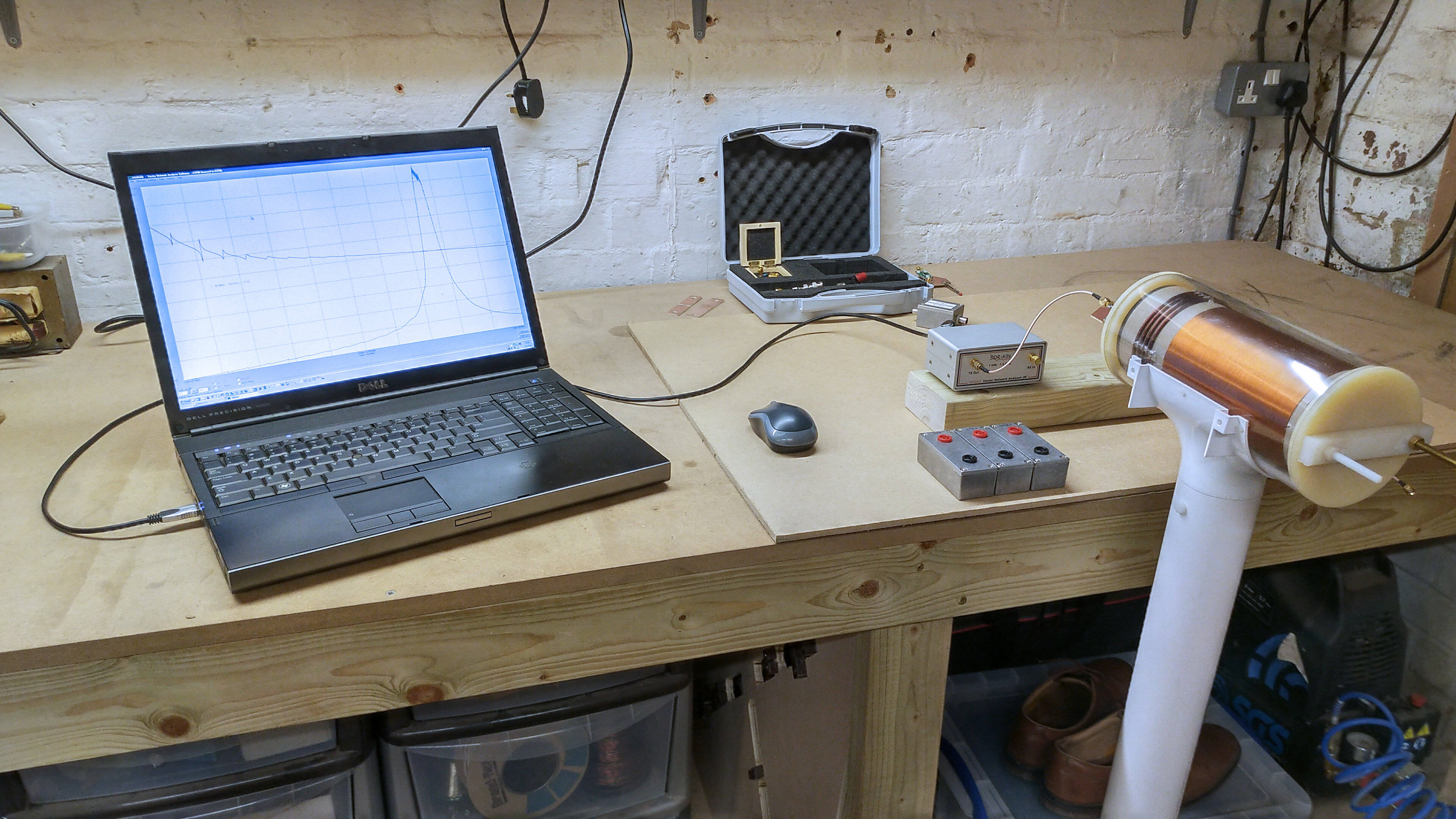
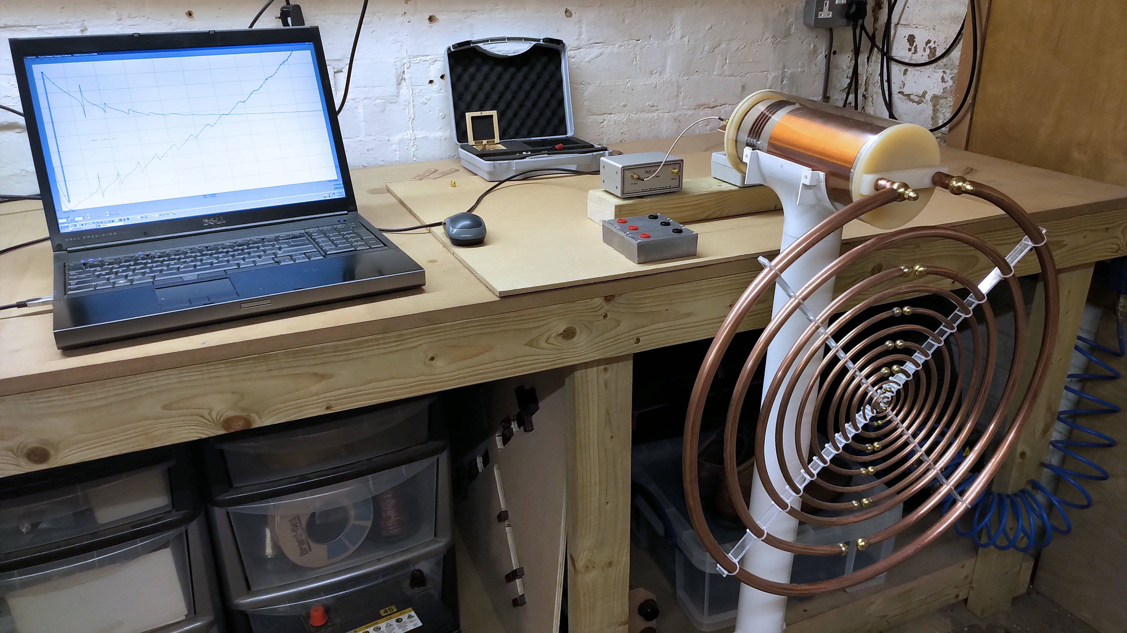
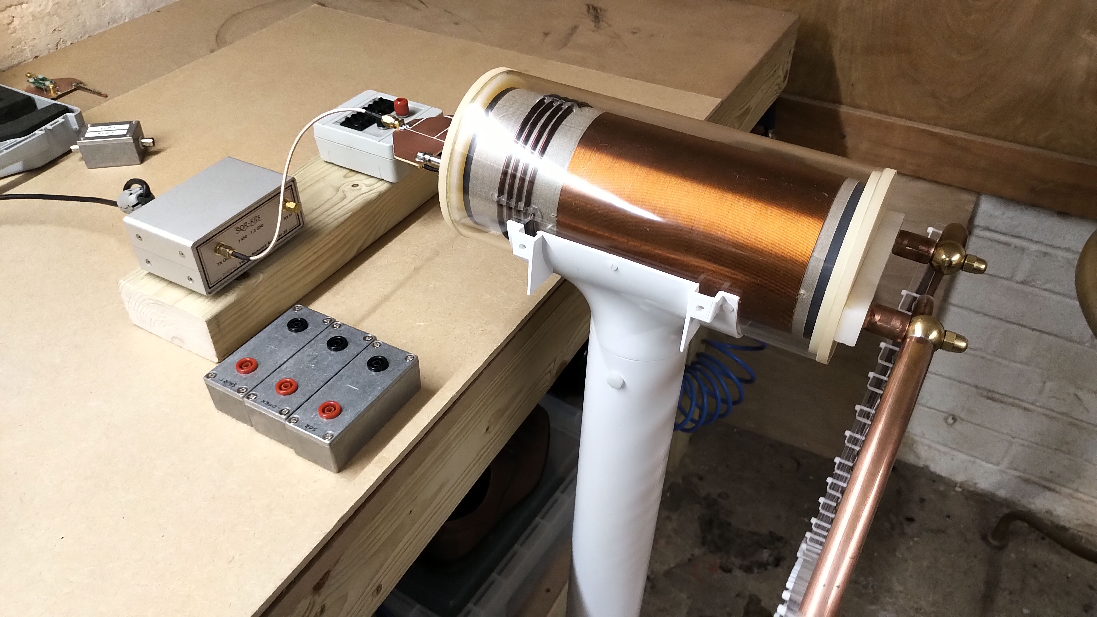
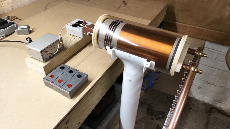
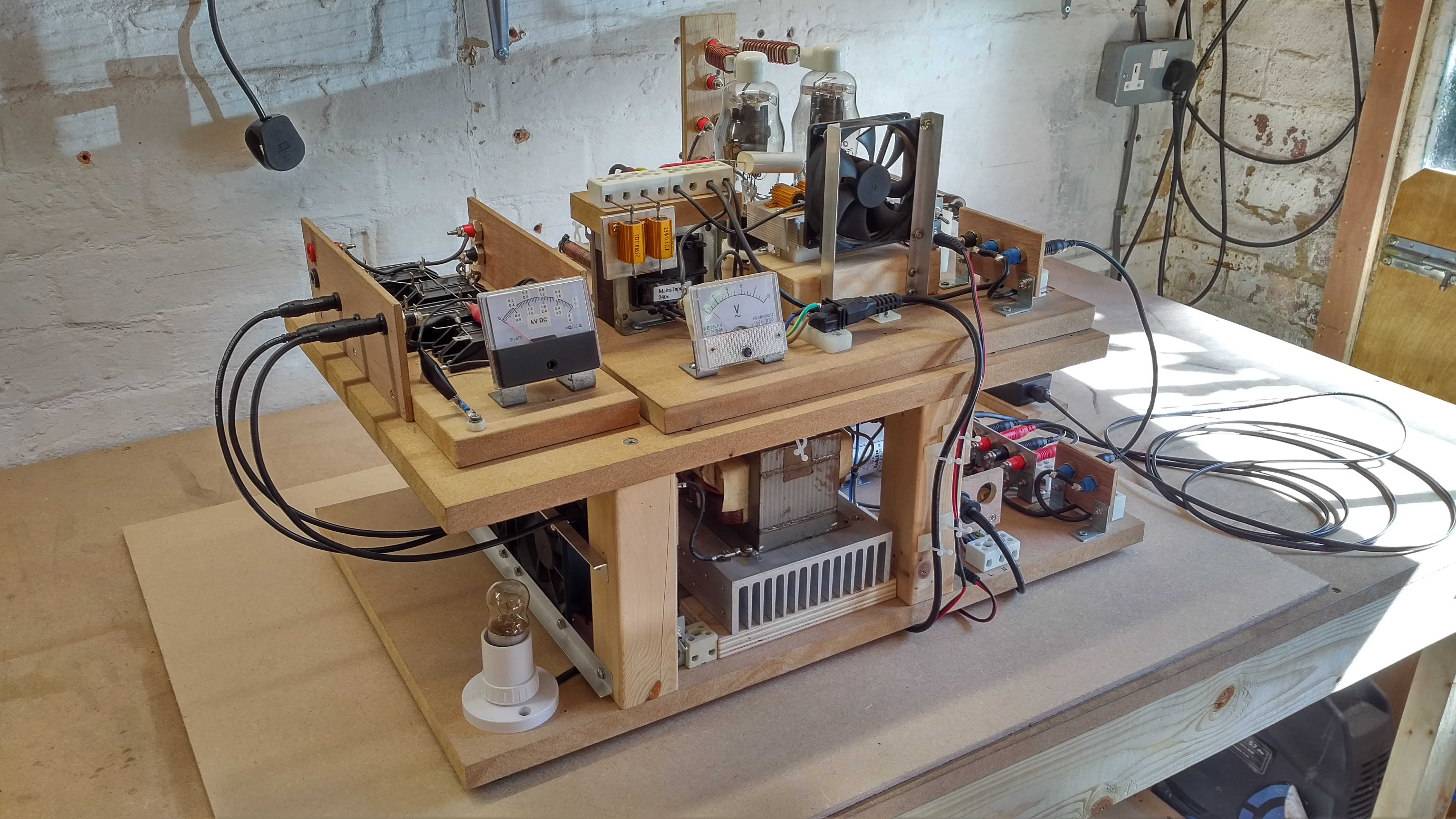
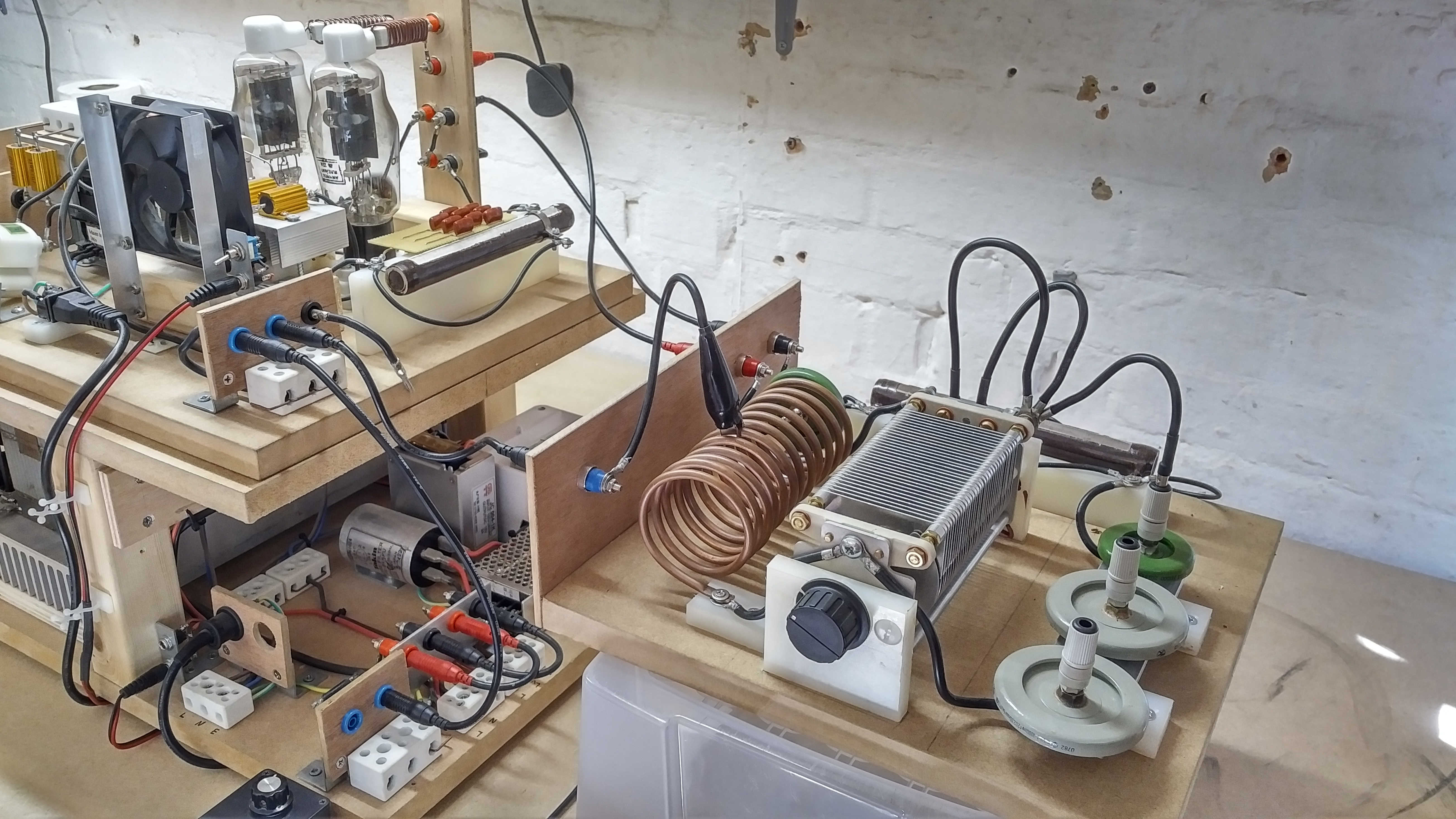
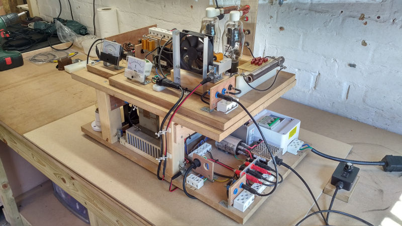
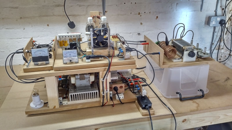
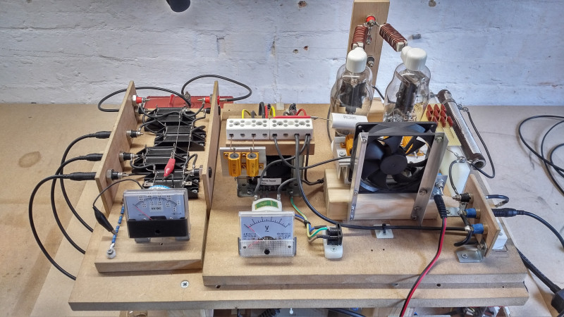
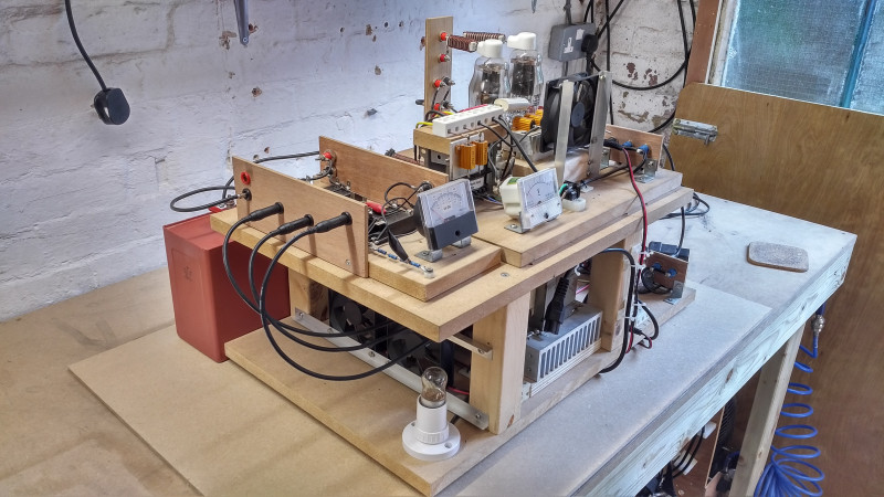
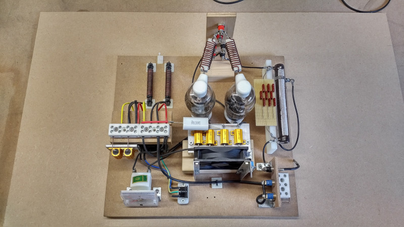
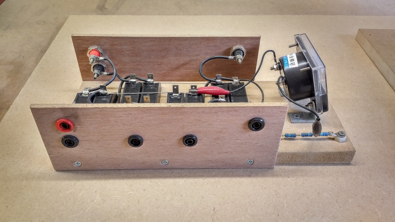
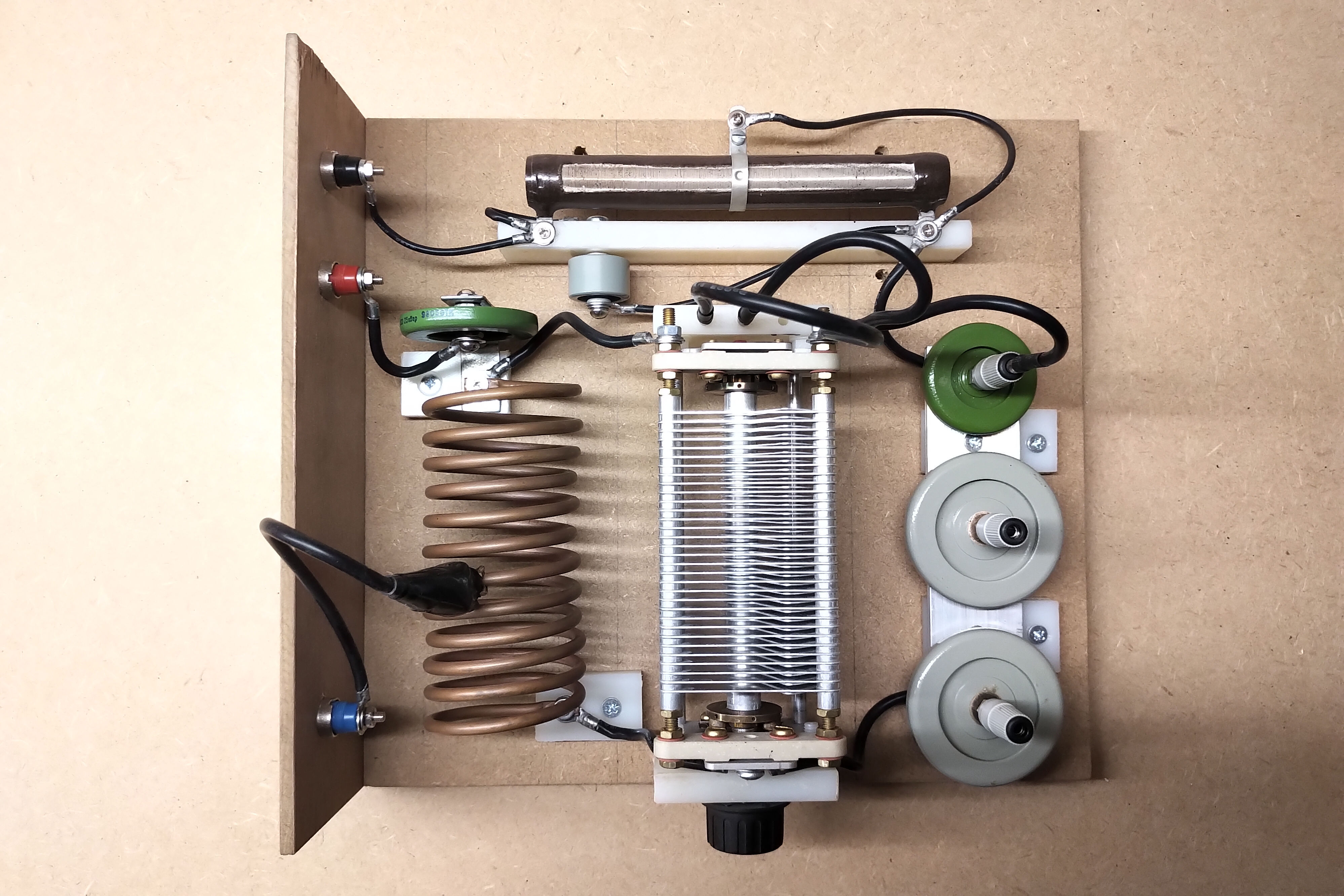
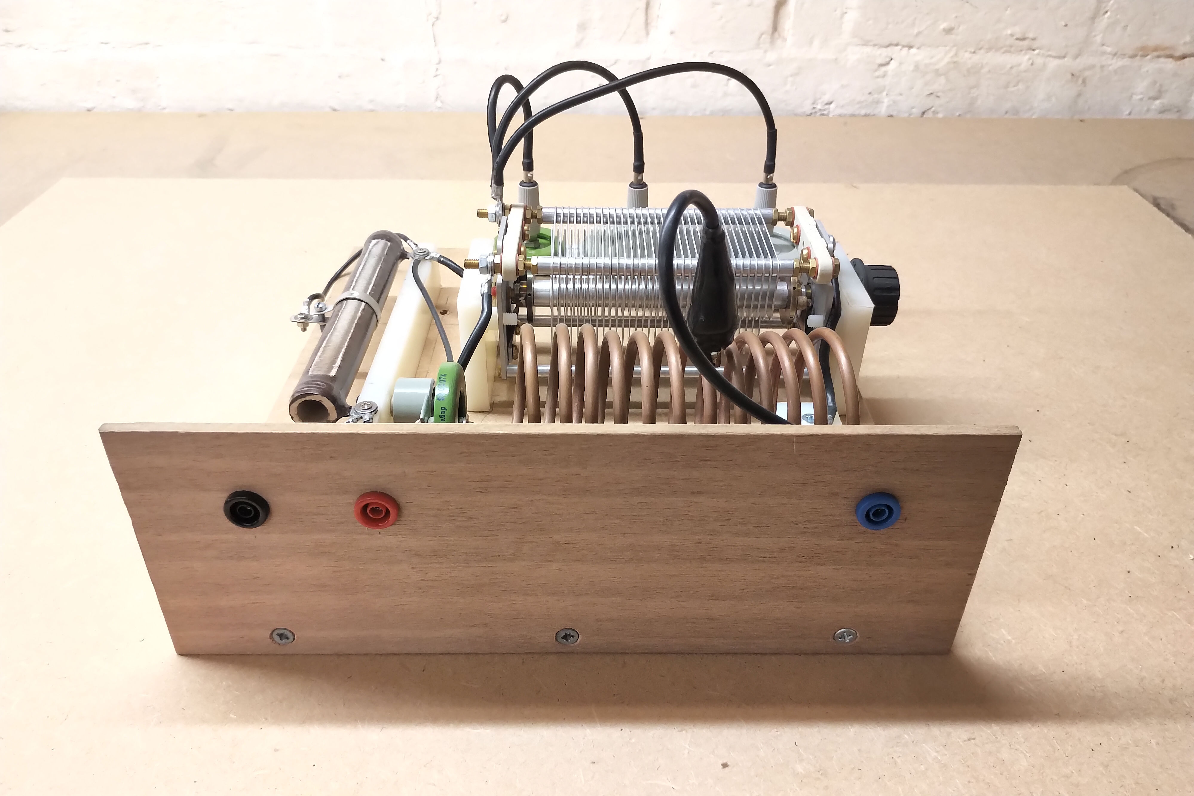
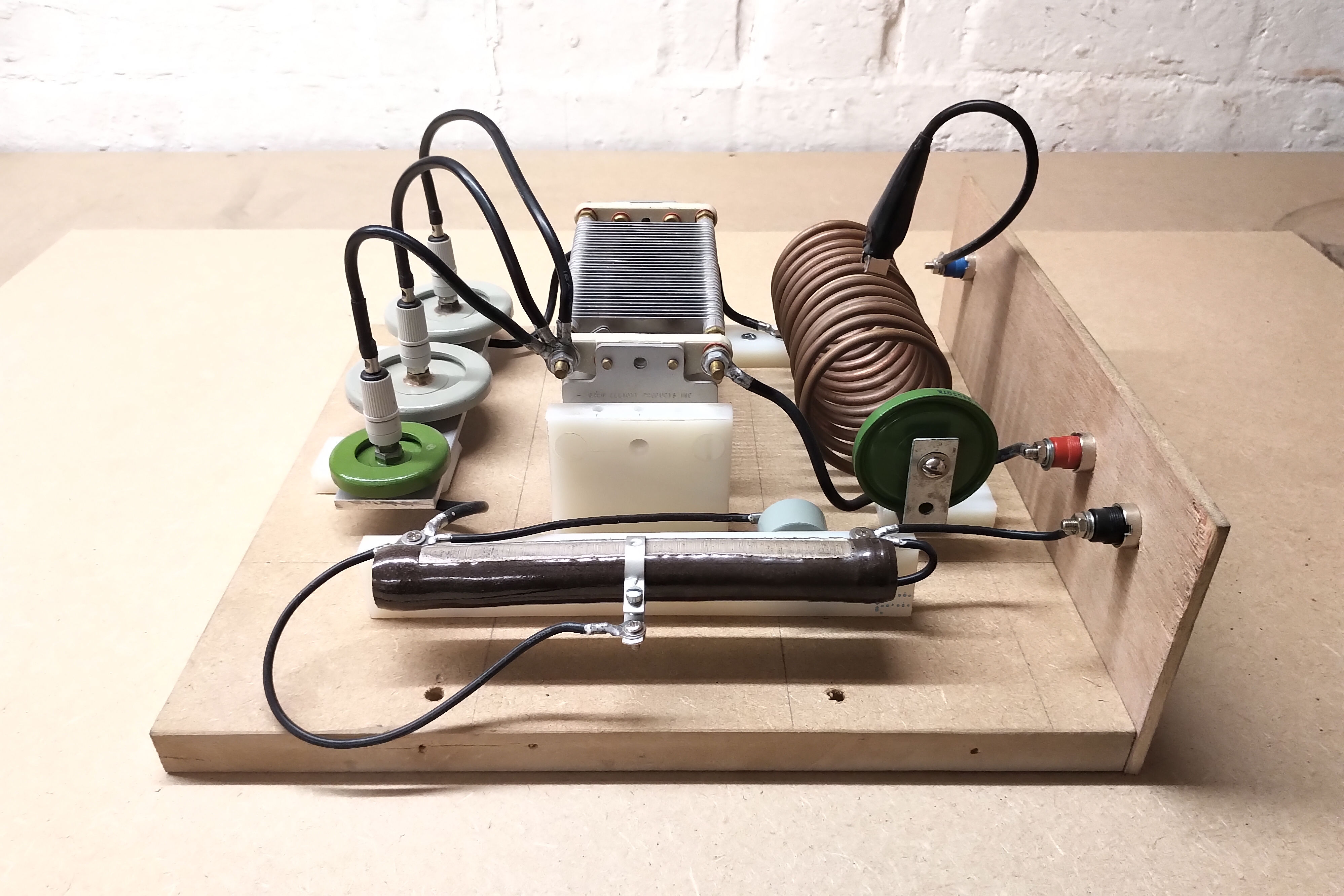
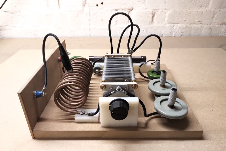
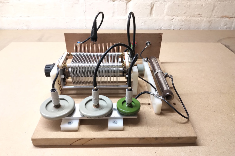
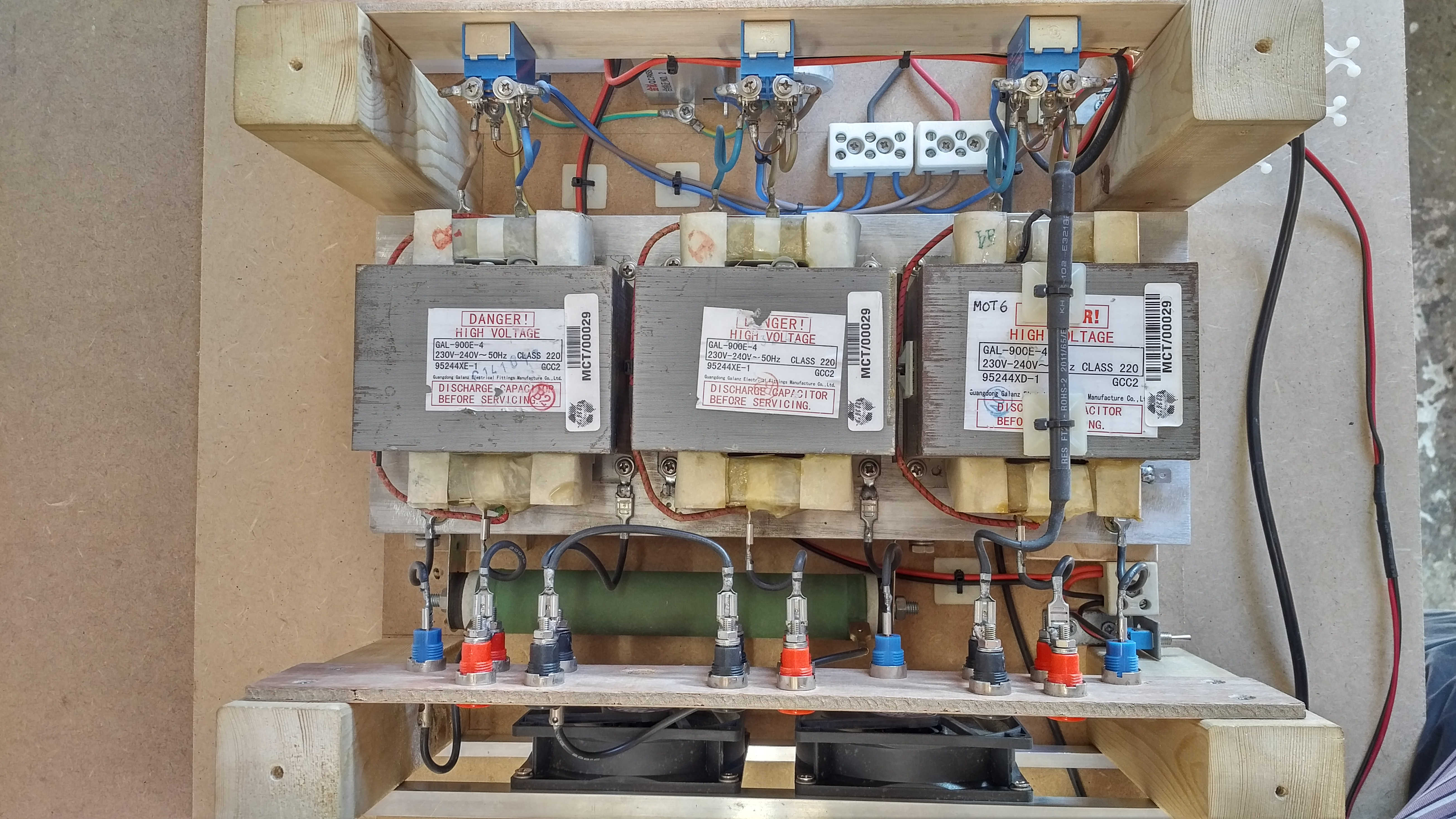
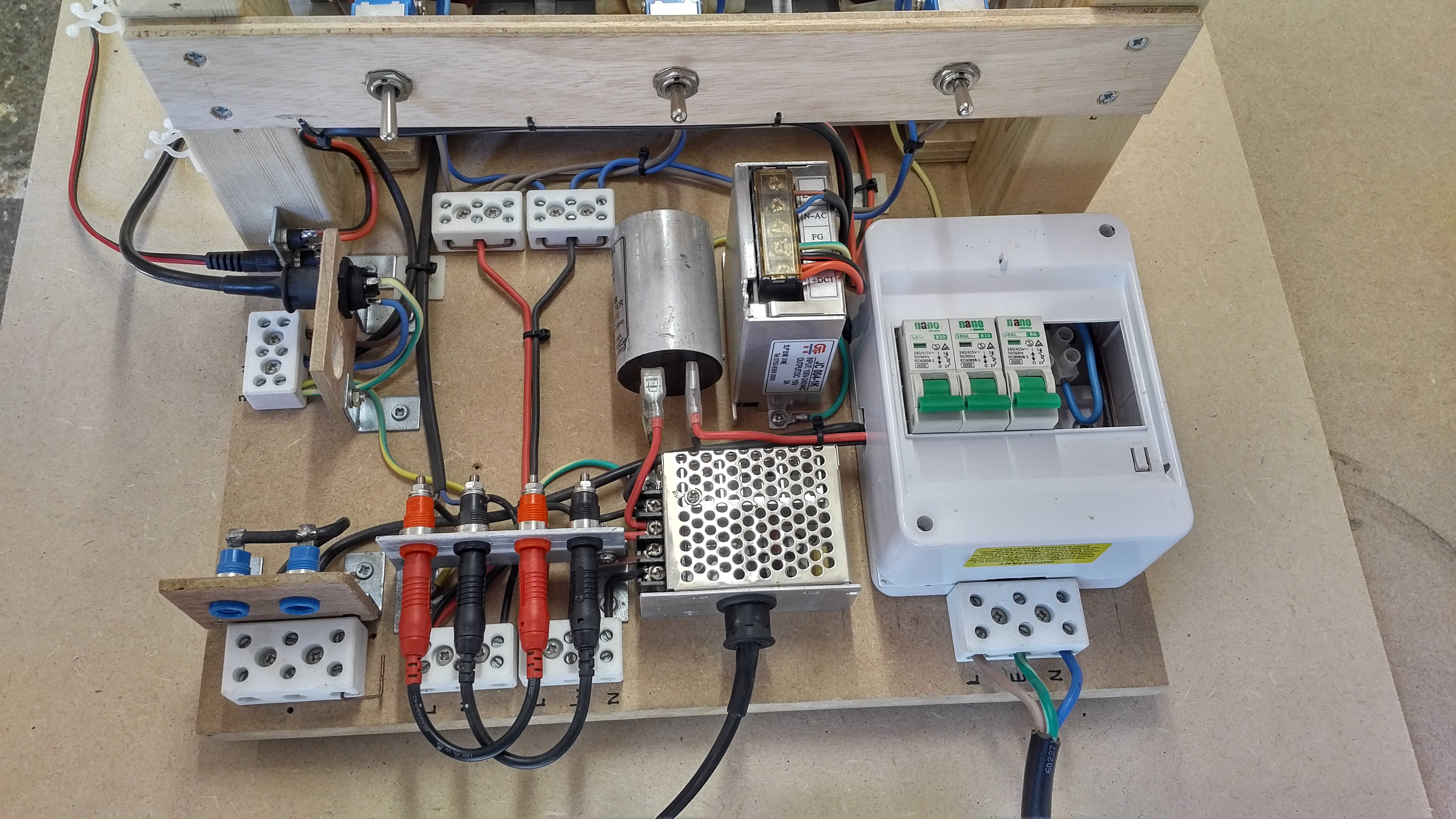
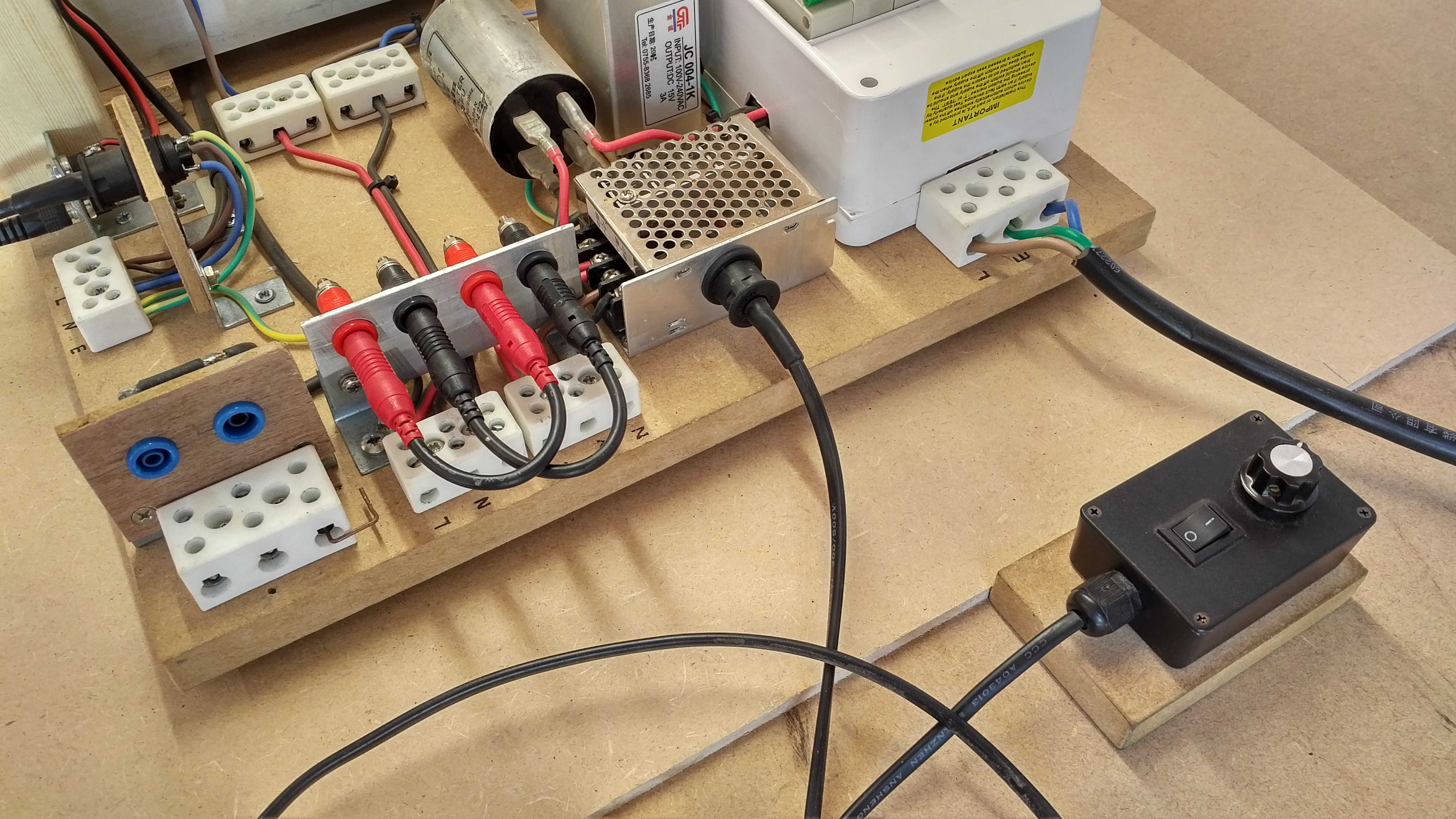
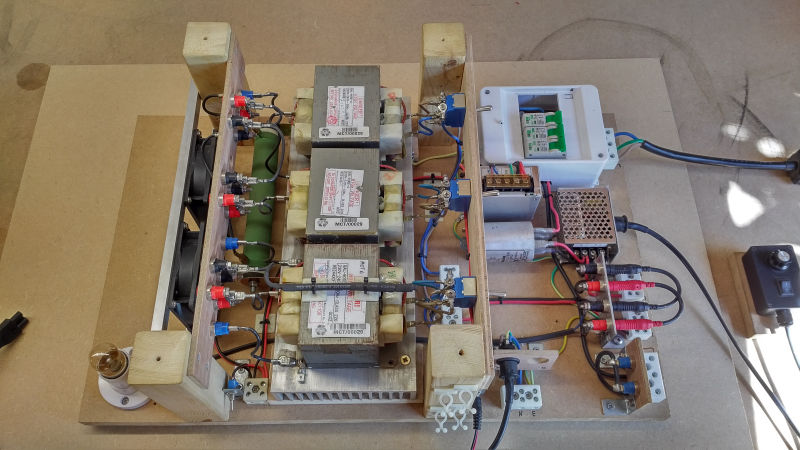
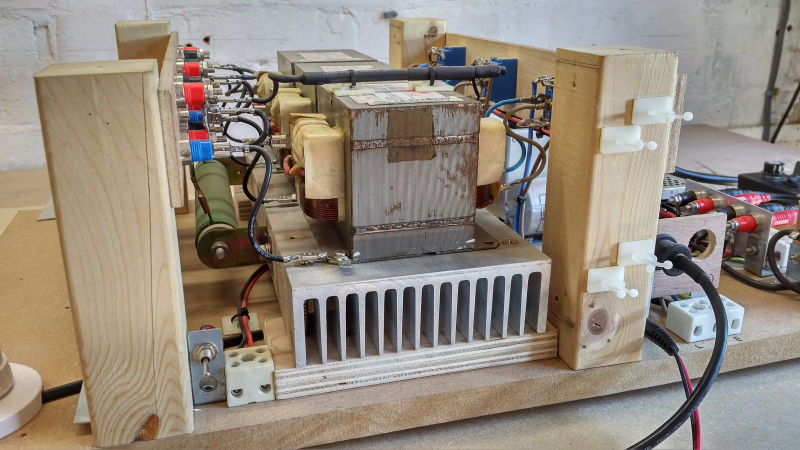
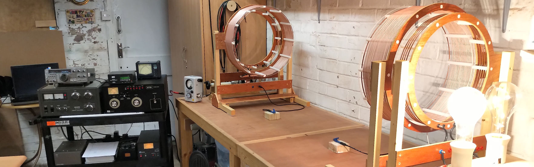
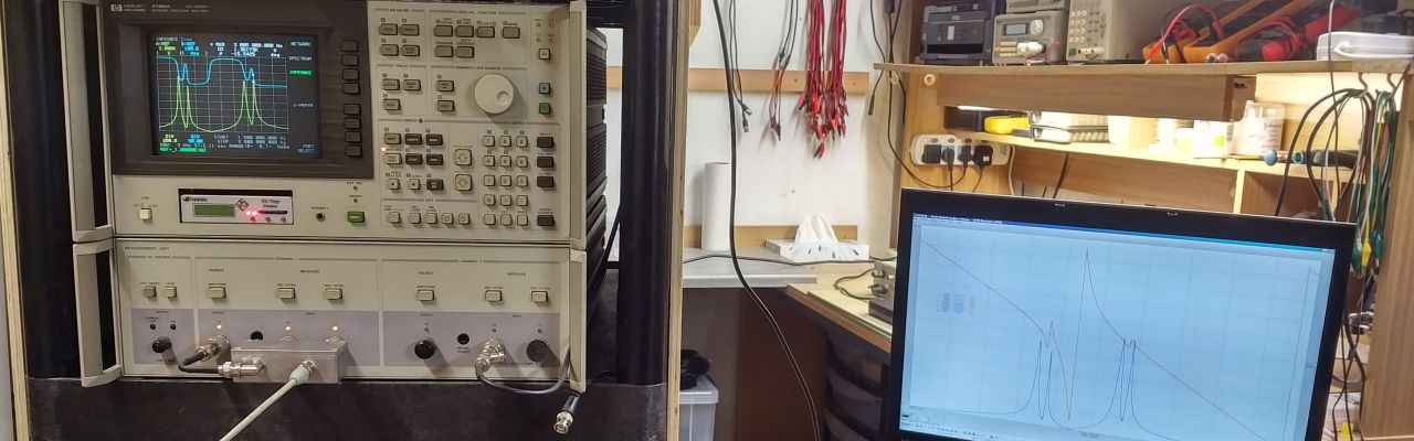
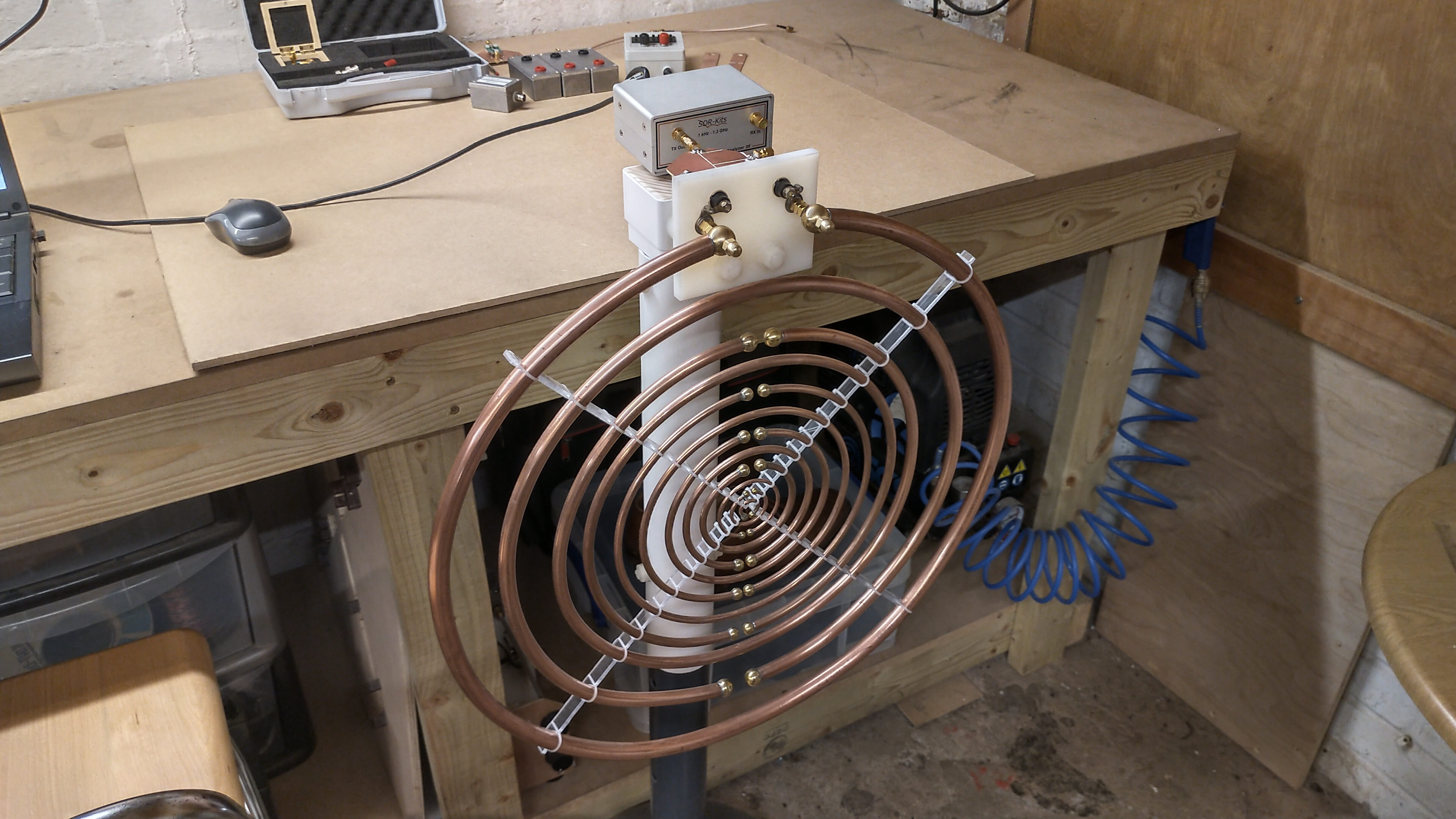
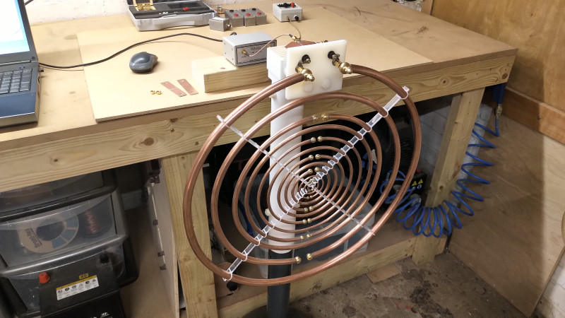
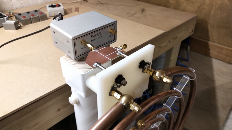
For this part, and to measure as accurately as possible Z11 for the MWO rings directly, and up to frequencies in the order of ~1Gc/s, it was necessary to make a connecting jig that allowed for extension of the reference plane from the VNA-SDR directly to the mounting spheres of the outer driven ring of the MWO. Figures 1 below show the measurement setup, signal feed adapter, MWO mounting jig, calibration elements, and overall arrangement of the high frequency impedance measurement apparatus.

To view the large images in a new window whilst reading the explanations click on the figure numbers below.

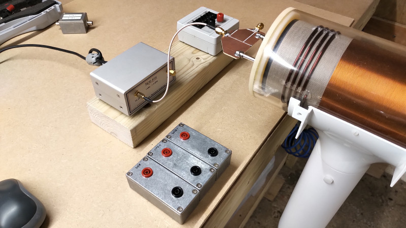
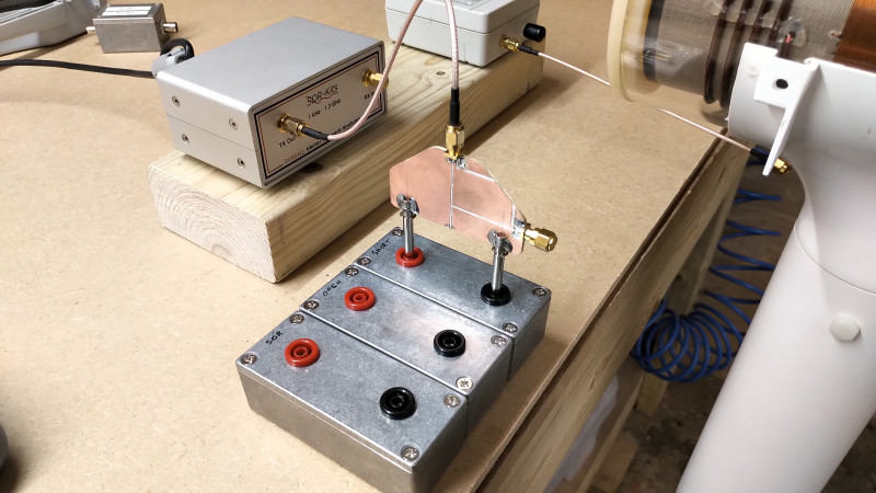
Fig 1.1. Shows the overall measurement setup with the VNA-SDR connected to the MWO mounting jig by a short SMA terminated RG316 cable, and the other end to the signal feed adapter (SFA), and standard calibration elements.

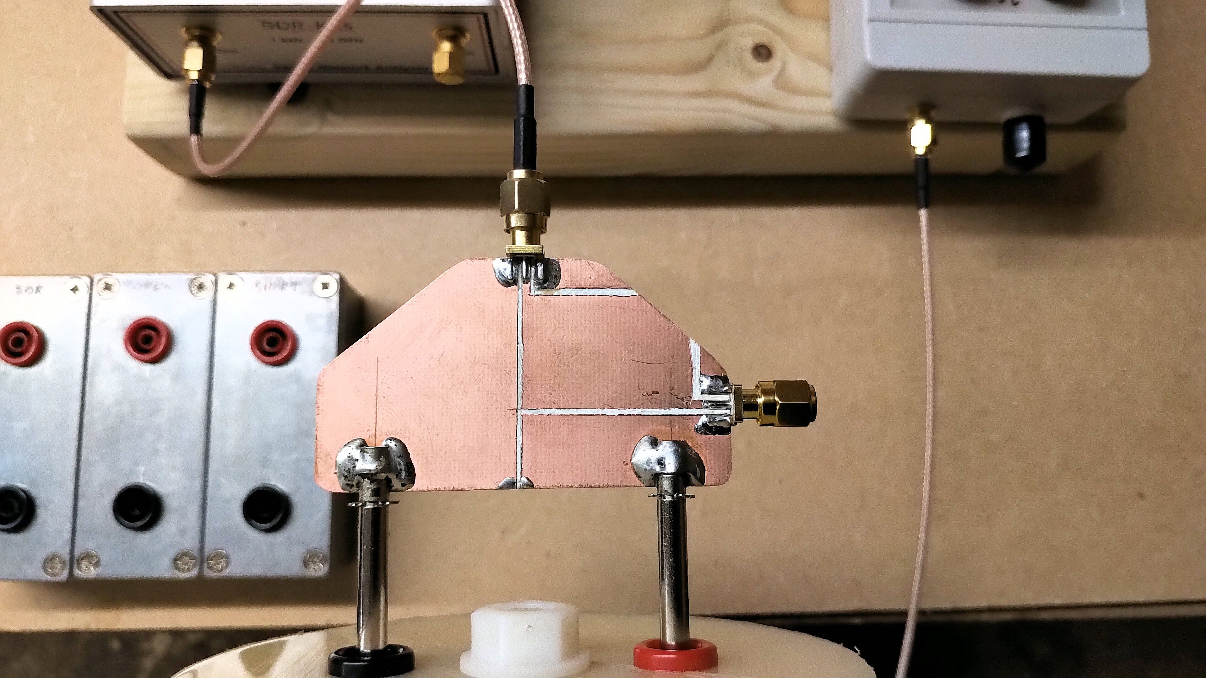
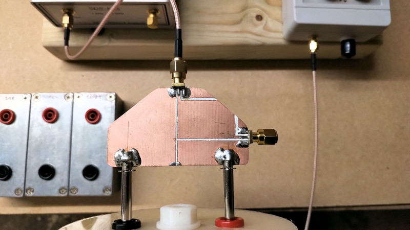
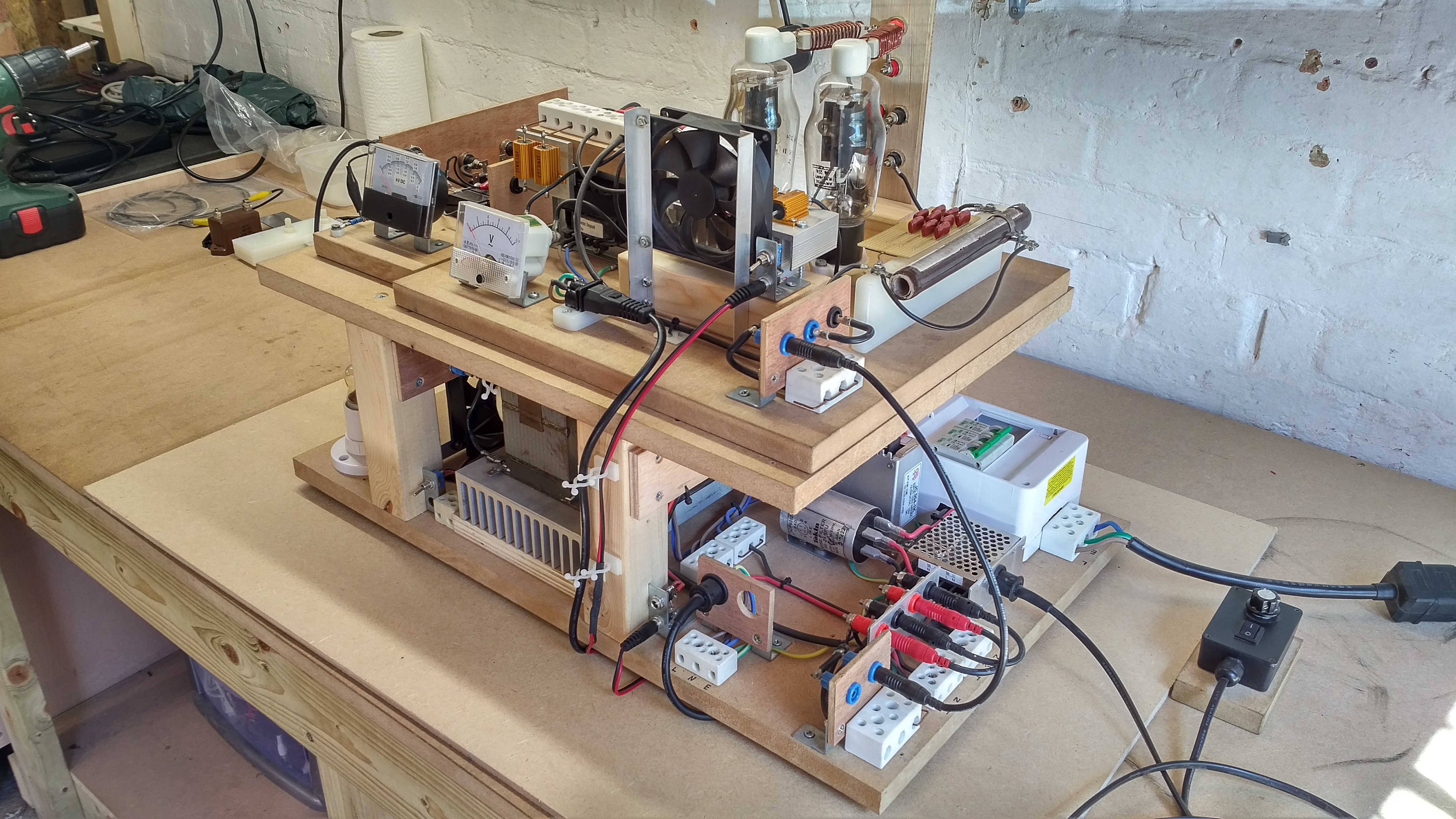
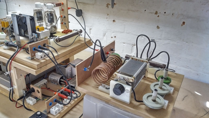
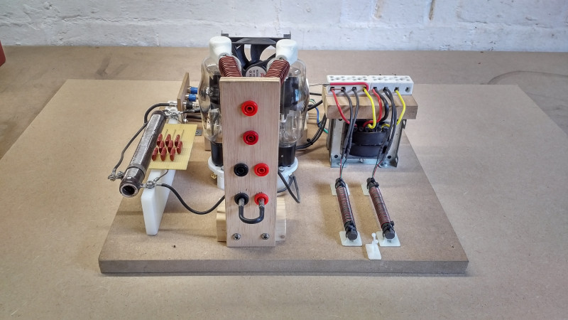
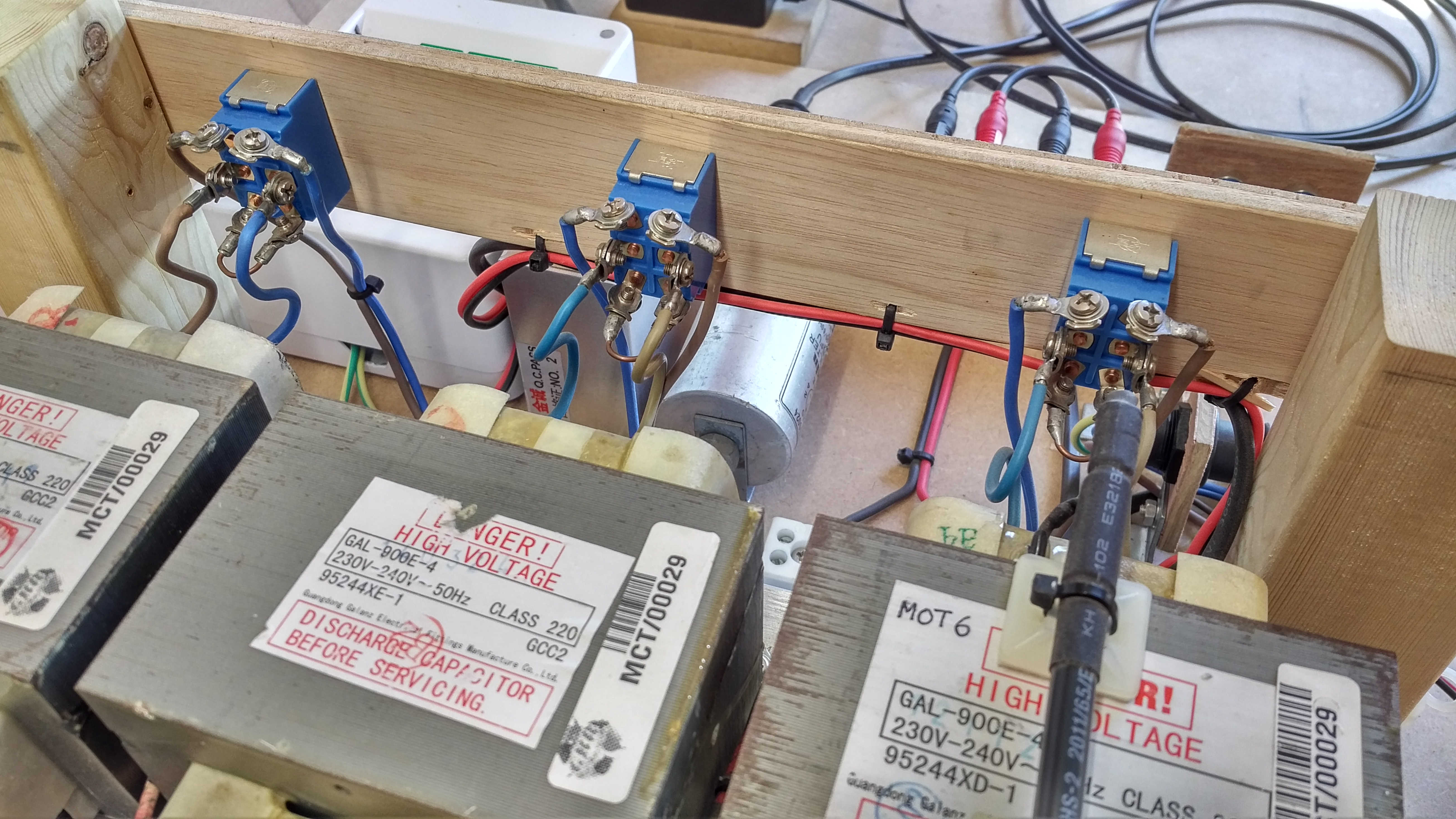
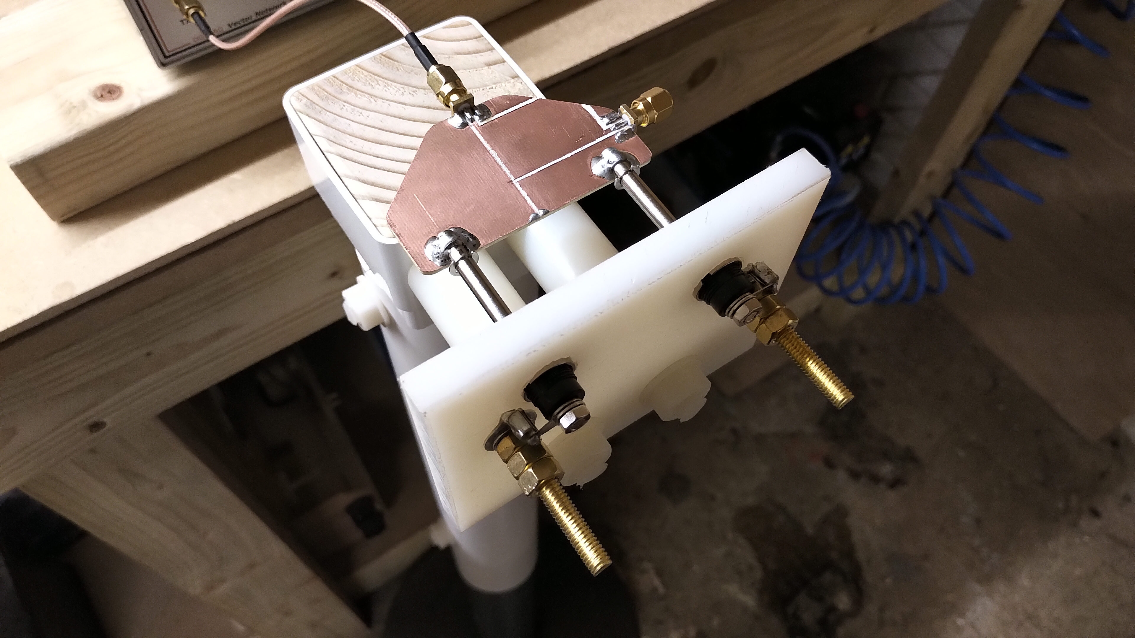
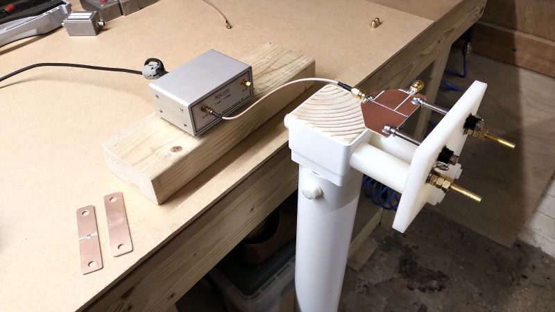
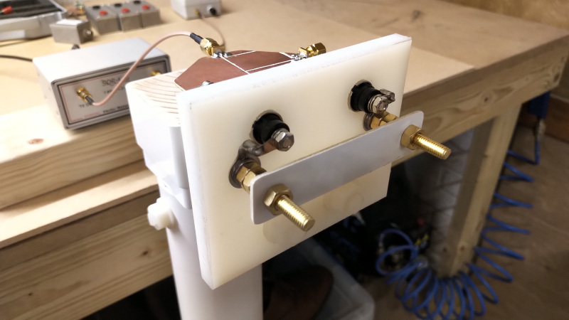
Fig 1.2. The SFA mounts directly to high voltage terminals, that are themselves connected to the brass mounting bolts used to hold the MWO rings to the jig. The jig is constructed predominantly in nylon 66 with a wooden internal support for strength inside the main jig support column. The high frequency path length and connection effects are normalised out by extending the calibration reference plane right to the brass bolt mounting points for the MWO outer ring. The SFA in this case is used with shorted series capacitance feed, and is balanced with equal weights of copper on the positive and negative feed paths, which includes the SMA connectors and the RG316 cable to the VNA-SDR. Equal weights of copper, or more accurately at high frequencies (> 3Mc/s), equal volumes of copper assist in balancing the boundary conditions for the electric and magnetic fields of induction and so reducing impedance mismatches in the signal feed path. As for part 1 an SFA with 3Gc/s balun was also tried but found to be largely unsuccessful in the small signal measurements due to the masking of high frequency detail, which results from the balun coupling transformer dominating the frequency characteristics in the mid to high-band frequencies.

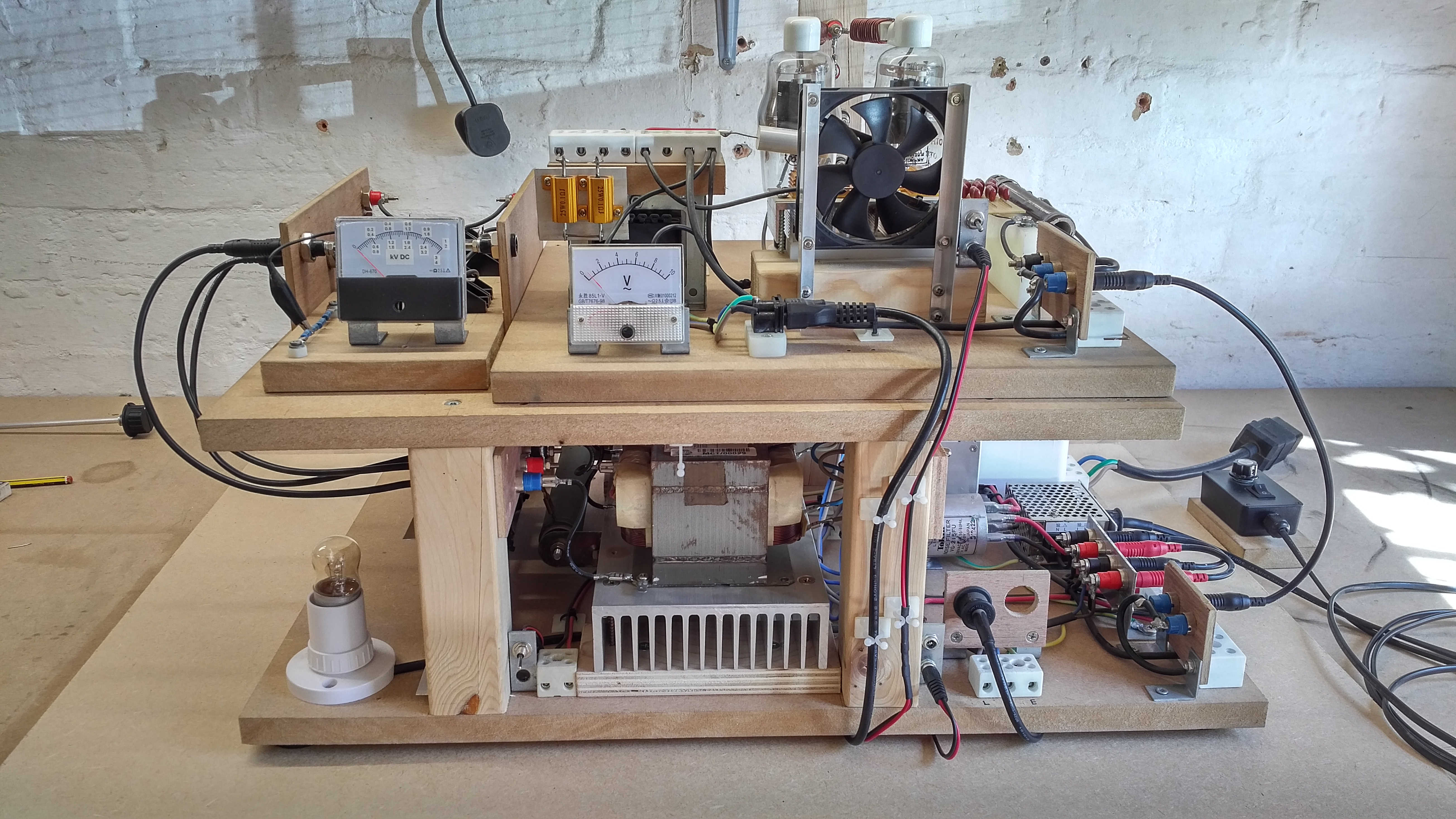
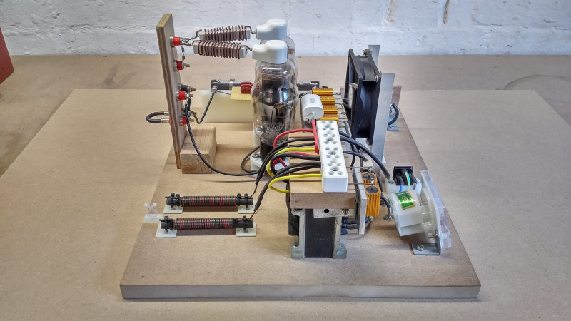
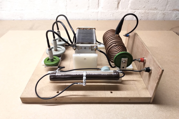
Fig 1.3. The calibration elements fit directly onto the end of the MWO brass mounting bolts. With no element attached the mounts are calibrated for open-circuit, a single-sided pcb element is used for the short-circuit, and a single-sided pcb with 50Ω surface mount resistor in the centre for the calibrated load.

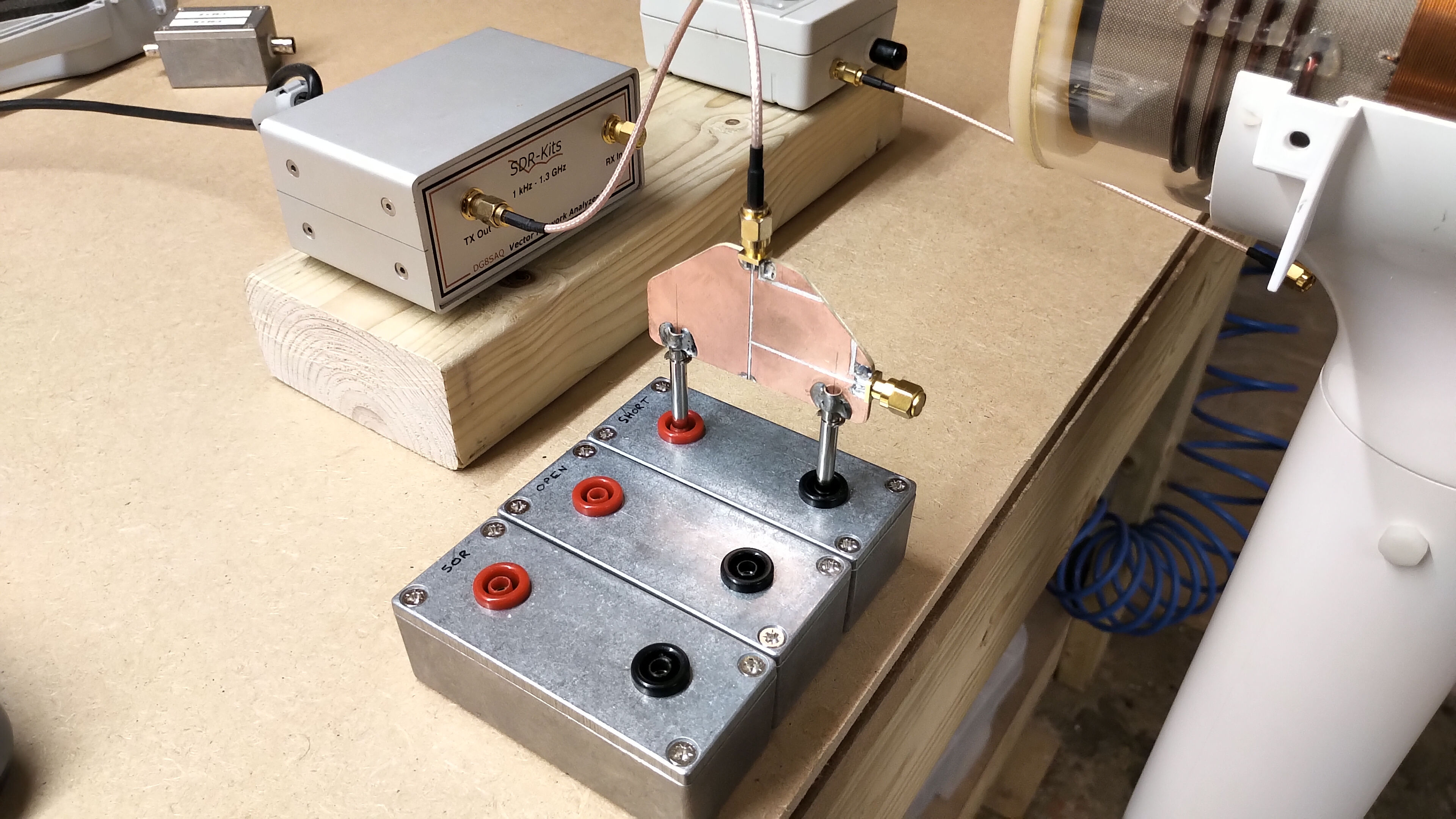
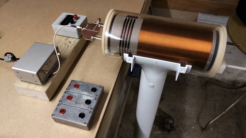
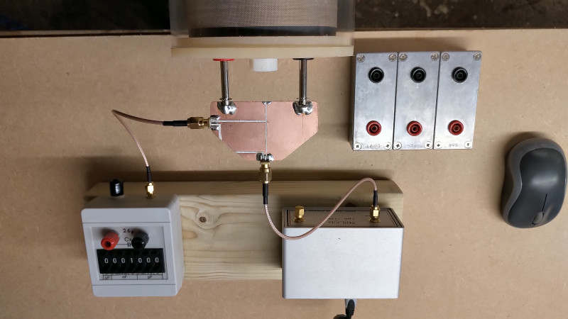
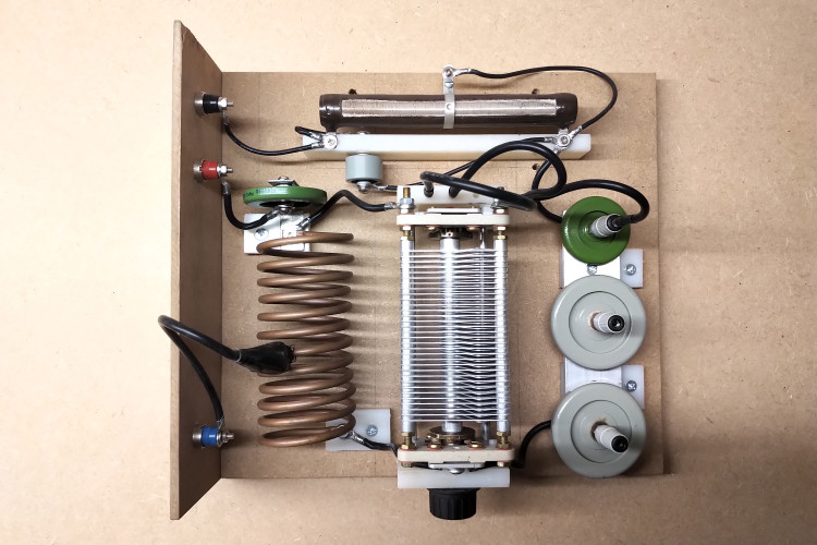
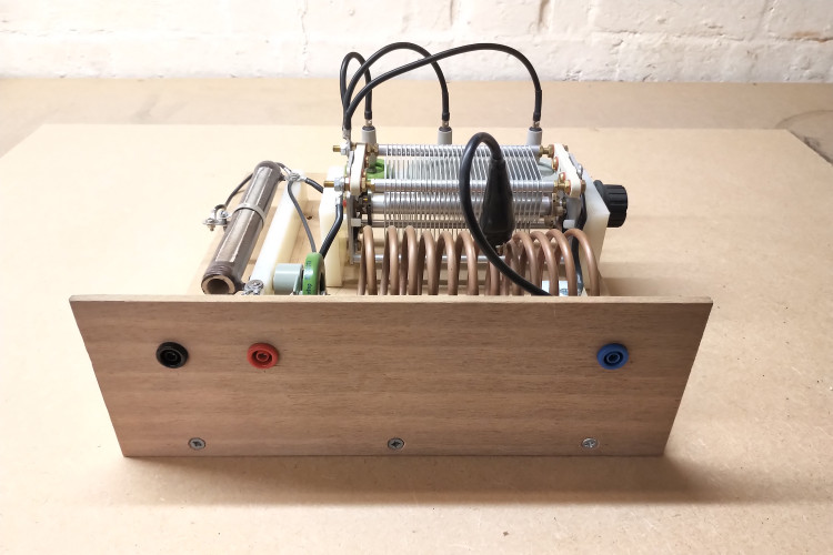
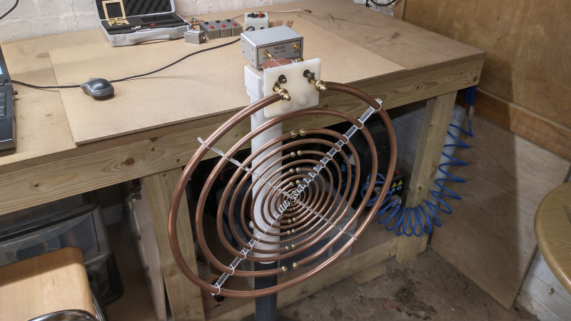
Fig 1.4. Shows the MWO rings mounted to the measurement jig.

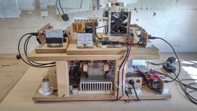
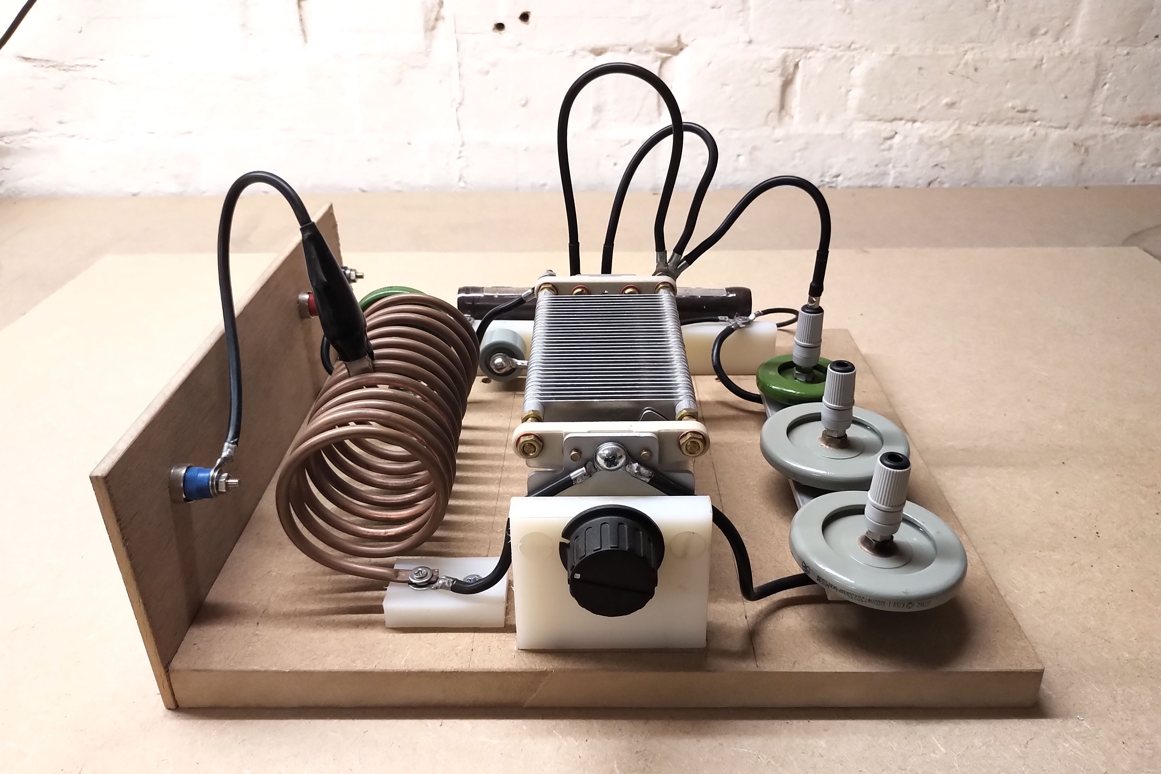
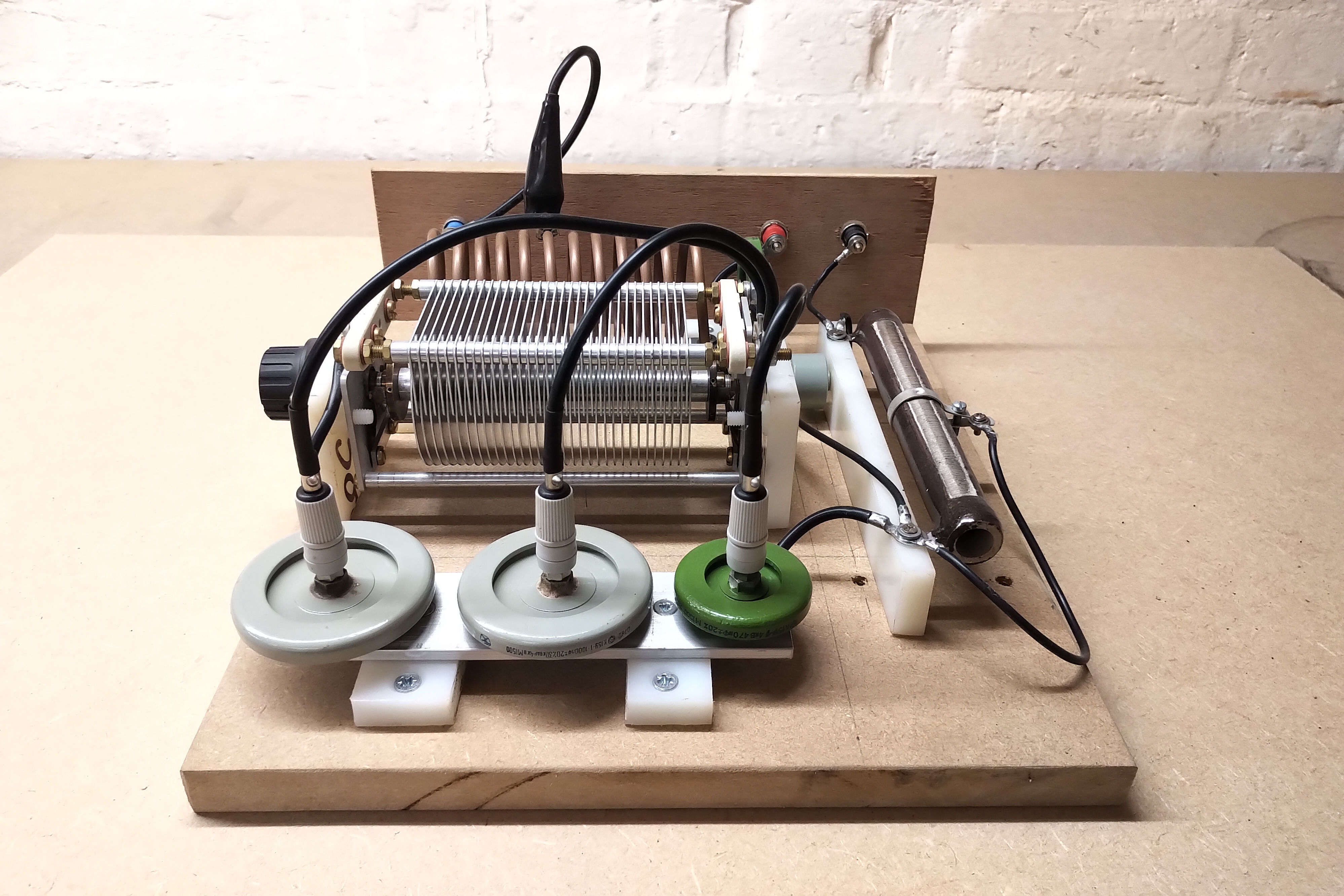
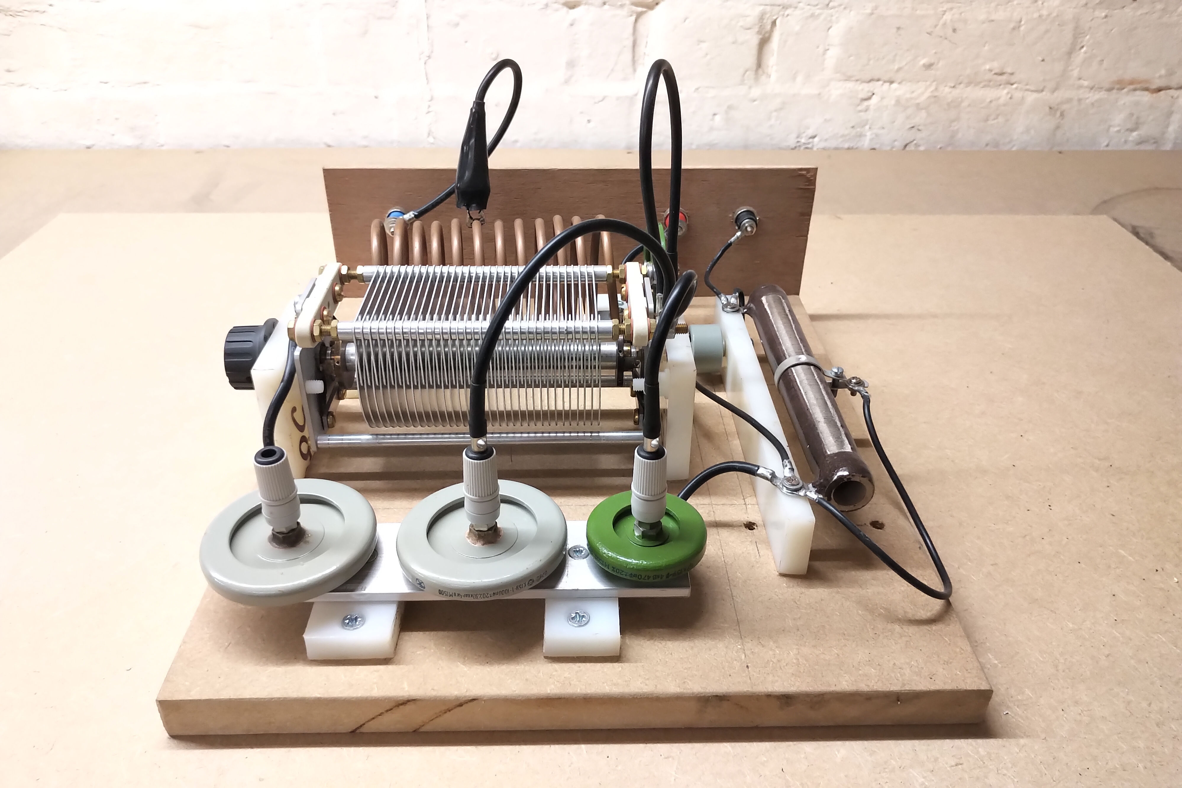
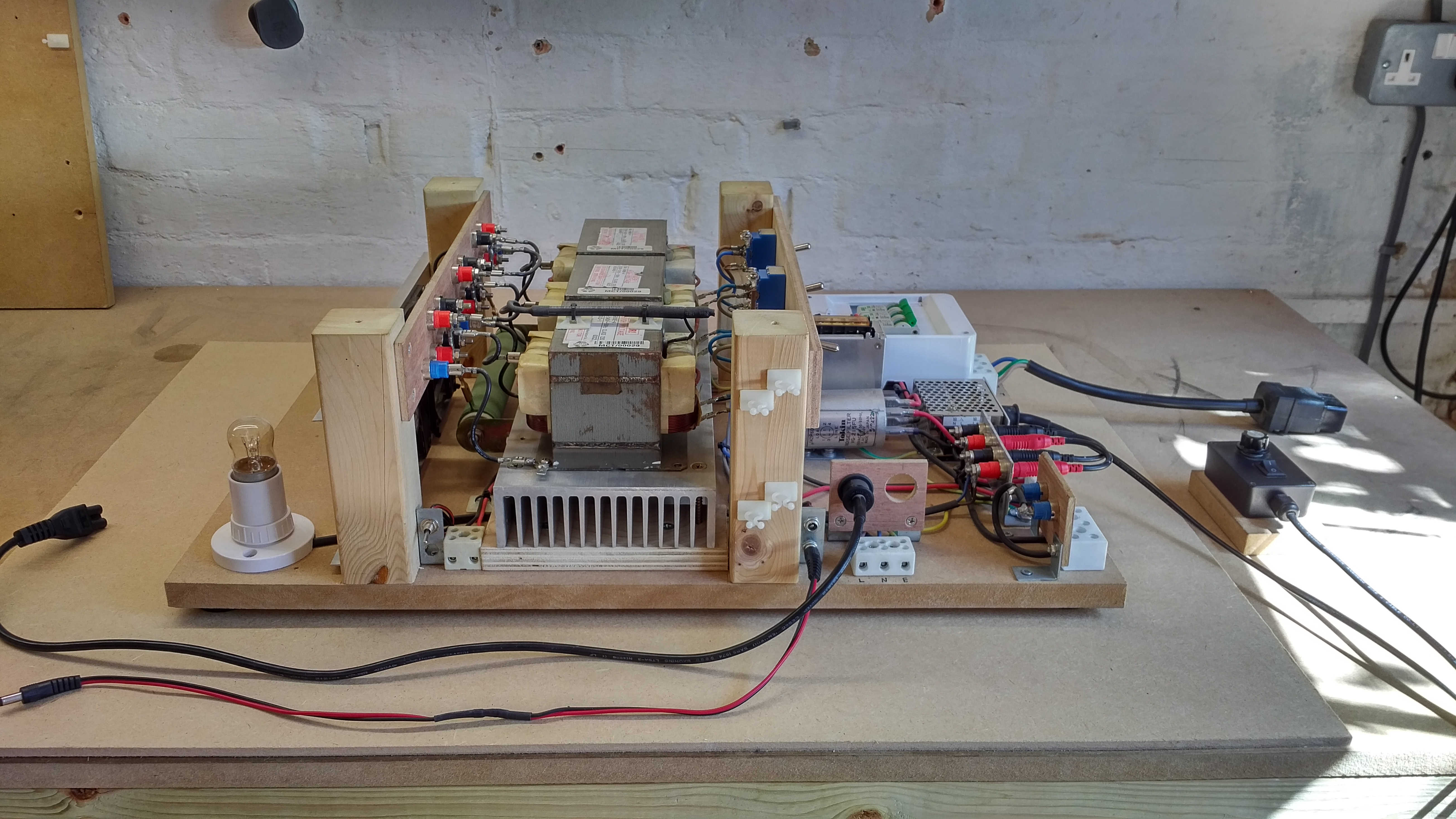
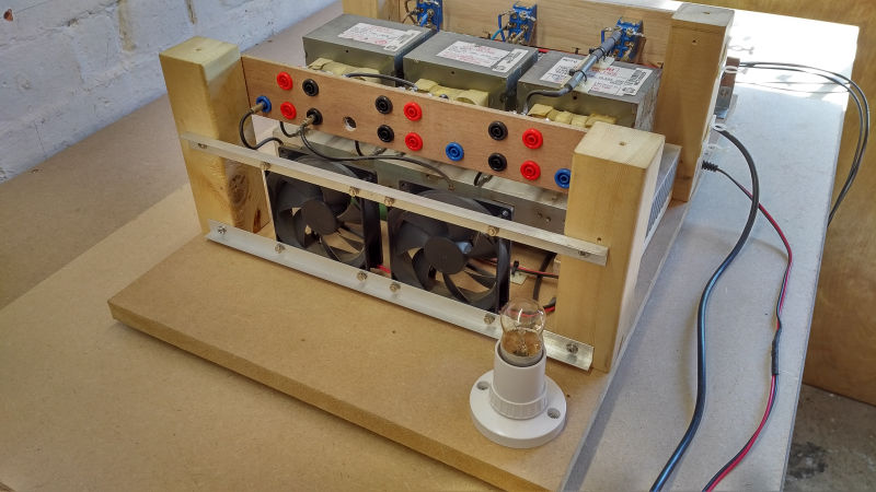
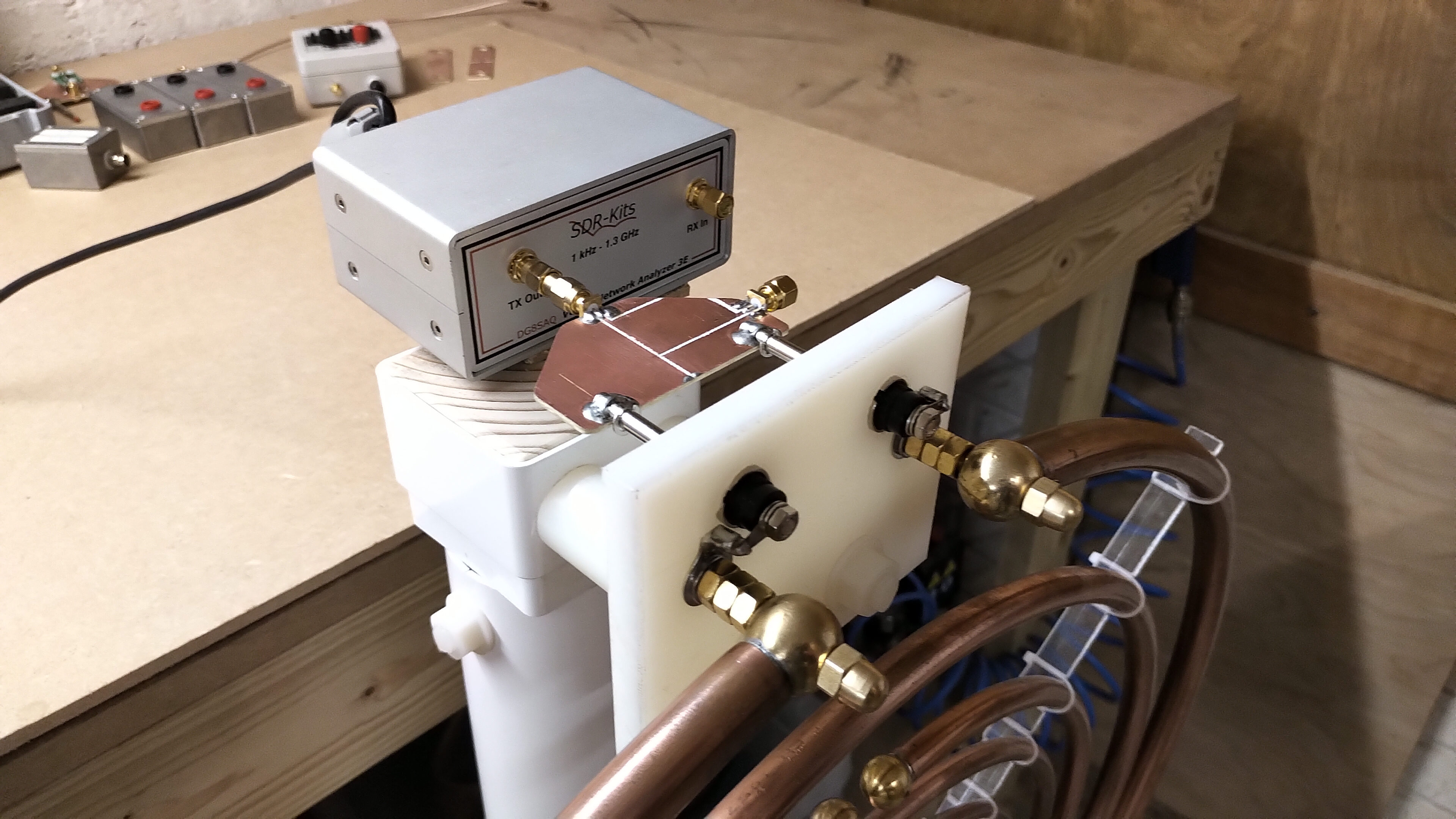
Fig 1.5. An improvement to the calibration procedure removed the SMA connecting cable by mounting the VNA-SDR directly to the SFA by SMA coupler. In this configuration some additional resonant features were removed from the normalised calibration results.

Fig 1.6. The final measurement setup for the high frequency MWO impedance measurements with VNA-SDR directly mounted to the SFA, which is in turn directly mounted to the jig, and where the calibration plane is at the point where the MWO outer ring brass balls meet the brass mounting bolts.

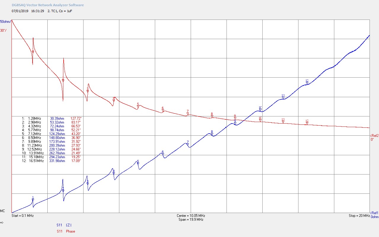
Figures 2 below show the Z11 impedance characteristics of the calibrated reference plane and the lower high frequency measurement band 100kc/s – 500Mc/s. The entire high frequency band was split into two in order to best comply with the calibration bands within the VNA-SDR instrument. At 500Mc/s the instrument internally changes reference method and level, and sensitive measurements cross-band are not recommended. Therefore the measurements are calibrated into a lower band 100kc/s-500Mc/s and an upper band 500Mc/s – 1.3Gc/s.

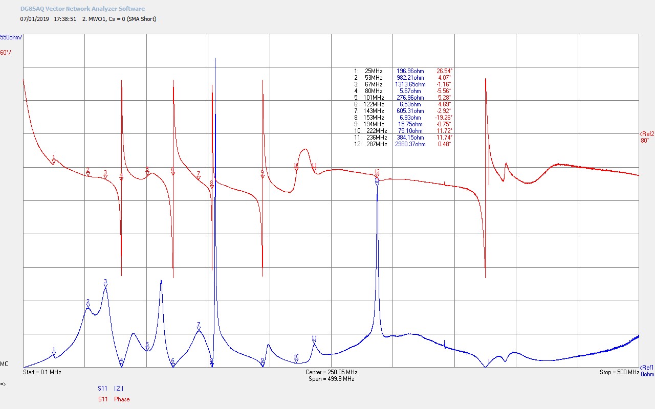
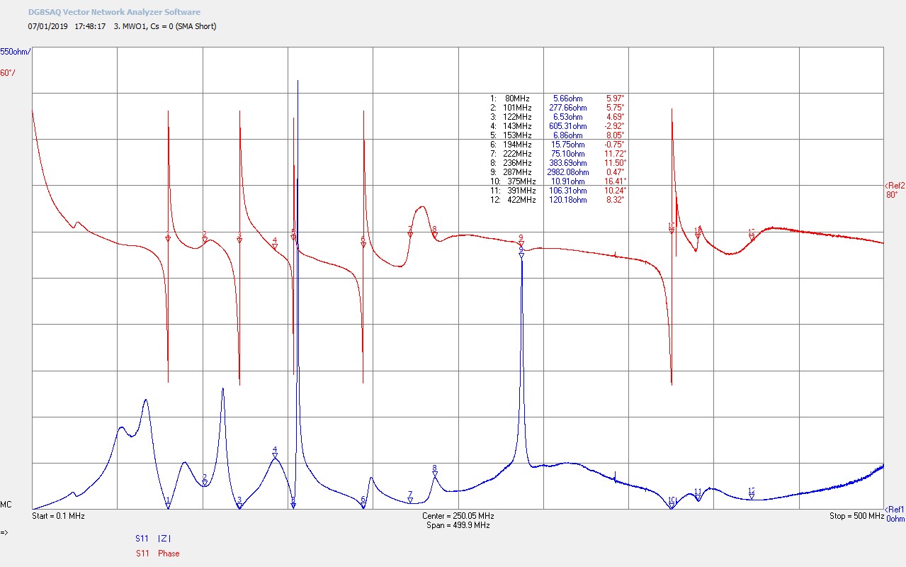
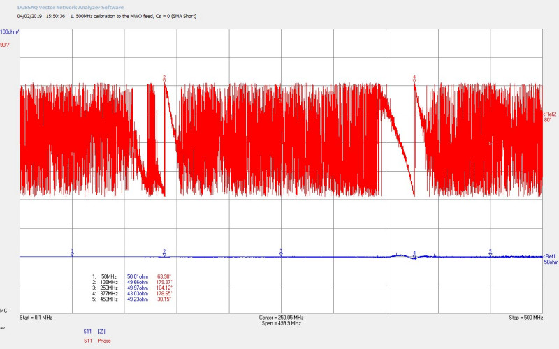
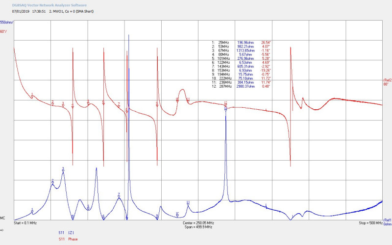
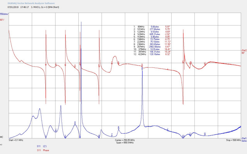
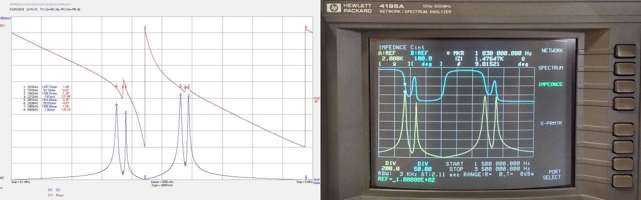
Fig 2.1. Calibration for the 50Ω reference element over the band. Markers M1, M3, and M5 show the consistent calibration across most parts of the band. At M2 at 138Mc/s and M4 at 377Mc/s there are resonances within the calibrated signal path which are too significant to normalise out. These points will need to be factored into the measurement results to remove features of interest, if any, that correspond at these frequencies. At these 2 points features in the results are considered measurement artefacts that arise due to the measurement system and inter-connection between the instrument and the MWO rings at the calibration plane.

Fig 2.2. Shows the rich range of resonant features that result from the MWO rings and their inter-action across the band. In this first result markers M1 – M12 are used to identify the lower 12 set of features, and in the next set of results the upper 12 set of features. There is no corresponding feature at 138Mc/s as seen in the calibration scan, and hence this point does not need to to be removed from the results. The first 250Mc/s of the results show a number of strong resonant points indicated by the large phase changes occurring at M4, M6, M8, and M9, and most likely attributed to resonances in the outer few rings of the MWO. There are also smaller phase inversions across the first half of the results occurring at M1, M2, M5, M7, M10, and M11 which most likely arise due to resonant inter-actions between the outer few rings of the MWO. At M12 287Mc/s  a large peak change in |Z11| occurs for a very small phase inversion, which would likely indicate where the outer drive ring of the MWO becomes self-resonant, in a similar way to that of the primary in the drive coil which becomes self-resonant at ~38MC/s. The point at M12 may also correspond to the 2nd harmonic of this point with the fundamental occurring at M8, this however being less likely due to the very low impedance swing at M8 to ~6.9Ω indicating that M8 is more likely to be associated with the fundamental resonance of one of the few outer rings, but not the driven ring.

Fig 2.3. Shows the markers on the upper 12 set of features. At M10 375Mc/s there is a large resonance, the only in the upper 250Mc/s of the results, which also very closely corresponds to the calibration feature noted in Fig 2.1. at M4 at 377Mc/s. The close correspondence of these two points means that the feature at M10 needs to be attributed to a strong resonance in the calibration path which could not effectively be normalised out by the calibration procedure. Otherwise in the upper part of the results there are some small phase inversions at M11 and M12 which could be tentatively linked to the fundamental resonant frequencies of some the rings further into the MWO centre. In the upper part of the results we start to see a general masking, smearing, and suppression of further detail, not necessarily because the detail is not there, but rather the coupling between rings is not sufficiently loose to allow for the natural resonance of each ring to be reflected in the results, and combined with rapidly increasing losses, large reductions in Q, and decreasing amplitude of oscillation as the results move towards the centre of the MWO. This could be further tested and measured by decreasing the coupling factor between each of the rings by changing the structure of the MWO from a flat set of rings to a cone configuration, where each of the rings retain the same diameter but are separated further apart vertically on the cone yielding a three-dimensional MWO structure. The other way to measure and assess this further is to remove every other ring in the flat MWO so reducing the coupling between rings and also reducing the large number of inter-active resonances. The process of starting with one ring inside the driven ring and subsequently adding ring by ring taking an impedance scan with each ring, would also assist in clarifying which fundamentals occur from which rings, and which features occur due to cross-coupling between the rings.

Figures 3 below show the Z11 impedance characteristics of the calibrated reference plane and the upper high frequency measurement band 500Mc/s – 1.3Gc/s.

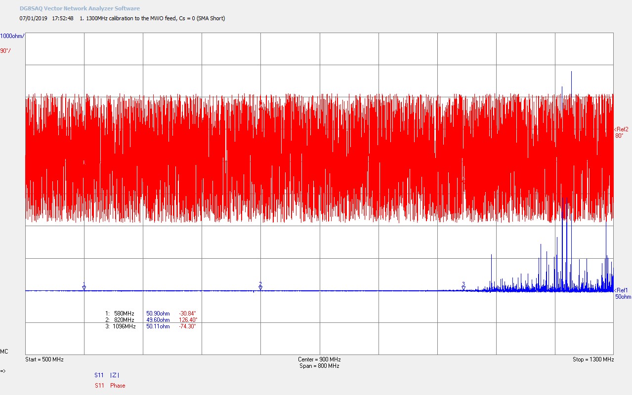
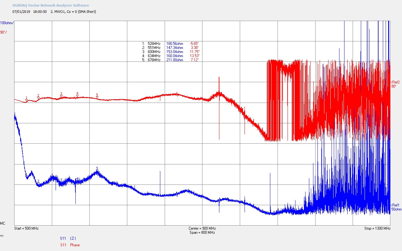
Fig 3.1. The calibration of the upper high frequency band shows very good consistency and results for the 50Ω reference load up to M3 at 1096Mc/s. Above this point the signal attenuation is such that the returned measurement currents to the VNA-SDR are so small as to be falling outside the lower dynamic range of the instrument, and hence the results become progressively more inaccurate and noisy. It is to be noted that the base 50Ω reference load can still be extrapolated visually to the end point ar 1300Mc/s. However, above ~1Gc/s the results on this measurement apparatus and setup are considered to not be of further use as can be more clearly seen in the next result.

Fig 3.2. At the lower end of this band markers M1 – M5 continue the upper band of the previous results in most likely showing fundamental resonances and maybe even some inter-actions between some of the more inner rings of the MWO e.g. rings 4-7. It is unlikely that any details can easily be discerned for the inner rings 8-11 where the signal reflections are very small, and stronger coupling between rings has largely smeared out the detail and suppressed the Q of the response.


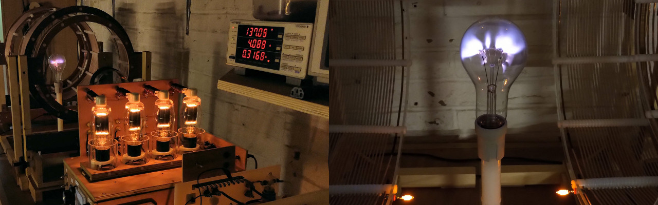
Overall the high frequency impedance measurements have presented a wealth of detail particularly in the lower part of the band and with discernible results being contributed to by as many as the first 6-8 rings inside the outer driven ring. It is also clear that cross-coupling between rings will contribute to very high frequency components to be emitted from the MWO, even though such detail is largely outside of the scope and dynamic range of the measurement technique used here. A useful comparison measurement would be to look at the range of frequency components generated during normal high tension operation of the complete MWO system, using a spectrum analyser instrument with capabilities into the Gc/s range. The high frequency impedance characteristics still need to be measured for the complete MWO system where both transmitter and receiver are connected to the system, which will be reported in a subsequent part.


1. Vril Science, Lahkovsky Multiwave Oscillator, 2019, Vril


Multiwave Oscillator Impedance – Part 1

The original Lahkovsky Multiwave Oscillator (MWO) apparatus combines two Tesla style drive coils in a transmitter and receiver configuration, each consisting of a primary and secondary coil cylindrically mounted on axis. The top-load for both transmitter and receiver is a complex combination of concentric half-wave resonators. The impedance characteristics of even a single drive coil with top-load represents a complex measurement challenge with results that can span over a very wide frequency range, in the order of 100kc/s – > 1Gc/s.

In this first part the small signal impedance characteristics, Z11 (magnitude and phase) with frequency as seen by the generator, are measured for a single drive coil both with and without the MWO top-load over the lower frequency range of 100kc/s – 20Mc/s. In this measurement the impedance characteristics are dominated by the drive coil which will mask any higher frequency measurements pertaining to the MWO top-load. For this reason the top-load is measured individually in part 2 in the frequency range 100kc/s – 1.3Gc/s. Subsequent parts will look at the overall MWO system impedance characteristics when both transmitter and receiver are combined together in the original Lahkovsky arrangement, and later in an optimised and balanced drive arrangement as designed and presented by Dollard[1].

In this first part the following measurements are presented:

1. Z11 (magnitude and phase) with frequency for a drive coil without MWO top-load in the range 100kc/s – 20Mc/s

2. Z11 for the drive coil combined with MWO top-load, and over the same frequency band.

3. Primary tuning measurements to match the resonant frequency of the primary coil, (with series loaded Cp), to the secondary coil at the fundamental, second, and third harmonics.

The SDR-Kits Vector Network Analyser 3E (VNA-SDR) was used to make all Z11 measurements, and the apparatus and method of measurement is shown in Figures 1 below.

To view the large images in a new window whilst reading the explanations click on the figure numbers below.

Fig 1.1. Shows the overall measurement setup with the VNA-SDR connected to the drive coil by a short SMA terminated RG316 cable, and the other end to the coil feed adapter, and standard calibration modules.

Fig 1.2. The drive coil used in these measurements has 4.5 primary turns of AWG 10 ~2.5mm diameter magnet wire, and the secondary has 248 turns of AWG 24 ~0.51mm diameter magnet wire. The top-end of the primary coil is connected directly to the bottom-end of the secondary coil and forms the negative or ground terminal. The positive or drive terminal is connected to the bottom-end of the primary coil, and the top-end of the secondary can be seen emerging from the coil through a brass bolt which attaches to the driven top-load. Both coils are wound anti-clockwise on the former from the base.

Fig 1.3. In order to make an accurate measurement of Z11 it is necessary to calibrate the VNA-SDR as close to the drive coil as possible. In this case the calibration plane is extended to the input of the primary coil terminals, (two 4mm high voltage shielded terminals), via a signal feed adapter pcb (SFA).  The SFA can be removed from the drive coil by drawing the two-pronged 4mm probes out of the drive coil terminals. With the SFA disconnected the VNA-SDR can be calibrated by fitting an open, short and 50Ω standard load to the end of the SFA. The effective calibration plane then becomes the input to the drive coil, and spurious impedance effects due to any cables and the SFA itself can be removed from the final results. When calibrated, a frequency scan of the SFA with the 50Ω standard load will show a flat impedance line for |Z|, (magnitude of the impedance). The phase of this scan will swing repeatedly between ±180° indicating the near perfect match between the calibration plane and the 50Ω standard load.

Fig 1.4. Shows a close-up of the SFA connected directly to the two high voltage drive terminals in the base of the drive coil. The SFA has an SMA input feed and is then connected via equal weights of copper to the series connection point. The black terminal indicates the negative or ground point where both primary and secondary are connected together, and the red terminal the high voltage feed end of the primary. The series connection point in the positive terminal allows for a calibrated capacitance box to be connected in the primary circuit for tuning measurements. In this picture the series connection is not being used and is terminated with a SMA short. In tuning measurements, when series capacitance CS is added, the SFA must first be calibrated with the capacitance box connected to the SFA with a nominal 1µF set at its output. The 1µF series capacitance has a very low impedance at the measurement band of interest and acts effectively as a short-circuit of the series connector during the calibration procedure. During tuning measurements the capacitance of the box is reduced in the range 100pF – ~ 50nF. The capacitance box itself uses surface mount standard capacitance values and can be reasonably used with SMA connection up to ~ 100Mc/s. The SFA is an unbalanced feed adapter and takes an unbalanced coaxial cable input directly to a balanced two terminal output without any compensation for this change in balance. A similar SFA was also tried which incorporated an RF (upto ~ 3Gc/s) balun in order to effect the transformation between the unbalanced and balanced connections. However, even with calibration the balun SFA proved to be less effective to measure Z11 accurately and cleanly, as it dominated the impedance changes in the frequency band masking changes due to the drive coil further downstream. The standard SFA was therefore used with careful calibration up to the intended reference plane at the input terminals to the coil.

Fig 1.5. Shows the calibration procedure where the SFA is connected in turn to the standard calibration modules, here connected to the short circuit module. In this case the series capacitance terminal is not being used and is shunted with an SMA short.

Fig 1.6. Shows the SFA in measurement configuration and after calibration, where a 1nF series capacitance is added to the primary feed. The calibrated capacitance box can be adjusted in 1pF increments in the range ~30.5pF –  ~10µF, where the parasitic capacitance of the box with SMA cable and when set to zero is ~30.5pF.

Fig 1.7. Shows the overall measurement setup with the top-load connected, and then calibrated and measured in the same procedure as previously discussed. The outer ring of the top-load forms an effective wire extension and capacitive load to the top of the secondary coil, which will both reduce considerably the fundamental resonant frequency and Q-factor of the drive coil. When compared with the drive coil without top-load the outer ring forms a λ/4 driven ring, which is coupling to 11 other λ/2 resonating rings. Given the size of the outer driven ring, and the proximity of the inner rings the coupling factor is considered to be quite high between the driven ring and the inner resonators, which will tend to constrain the free resonation of the inner rings and considerably quench the Q and hence measurements at much higher frequency. This is considered more closely in part 2.

Fig 1.8. Shows in more detail the mounting points at the top-end of the secondary and the MWO top-load.

Figures 2 below show the Z11 impedance characteristics of the calibrated reference plane, the drive coil, and primary and secondary tuning with series added capacitance, of the drive coil only.

Fig 2.1. Shows the calibrated reference plane of the SFA when connected to the 50Ω standard load over the wideband range 100kc/s – 20Mc/s. The calibration is as expected and accurate over the band, with a slight phase variation between ~ 3 – 3.5Mc/s indicating a resonance in the signal path between the calibration plane and the VNA-SDR which has been normalised out by the calibration procedure.

Fig 2.2. The impedance characteristics of the drive coil with the series capacitance Cs = 1µF, showing a wealth of resonant peaks and corresponding phase changes from the fundamental resonant frequency FS of the secondary coil at 1.28Mc/s up to the 12th harmonic FS12 (M12) at 16.51Mc/s. It is interesting to note that the 2nd harmonic FS2 at M2 is a stronger resonance than that of the fundamental at M1. This is further demonstrated in subsequent impedance results. The VNA-SDR allows for only 12 concurrent markers which is why the final two harmonics on the results are not marked. At frequencies above 20Mc/s the rapidly increasing inductive impedance of the primary masks out any further harmonic points of interest, and the impedance curve rises rapidly until the primary coil becomes self-resonant at ~38Mc/s.

Fig 2.3. Shows the calibrated reference plane of the SFA when connected to the 50Ω standard load over the narrowband range 100kc/s – 5Mc/s. With more accurate calibration in the narrowband it can be noted that the phase variation seen in Fig. 2.1 has now been completely normalised out of the reference plane.

Fig 2.4. Shows the narrowband impedance characteristics for the fundamental FS and the first two harmonics FS2 and FS3. Here the difference in magnitude of the resonance between FS and FS2 can be very clearly observed, although the Q of the coil remains very similar for both frequency points. The magnitude of the impedance |Z11| ~ 28.5Ω at FS, and ~ 49.7Ω at FS2 would significantly impede currents developed in the primary from the generator, coupling very little power to the secondary and ultimately to the MWO top-load. The primary circuit will need to be brought into resonance with the secondary at the corresponding frequency in order to considerably reduce the driving impedance seen by the generator, and hence maximise the primary currents, and the amount of power transferred from the generator through the drive coils to the top-load. On the very far left of the scan at 100kc/s the 180° phase change FØ180 of the primary in resonance with the series capacitance CS can just be observed. This will be adjusted by varying CS in subsequent results in order to tune the primary resonant frequency to that of the secondary. Given the difference in magnitude between the fundamental at FS and the 2nd harmonic at FS2 it may be more optimal to arrange the primary to resonate at FS2 rather than the fundamental for normal experimental operation. This will be tested during experiments and reported in subsequent parts.

Fig 2.5. Here the series capacitance CS has been reduced from 1µF to 400pF which has increased FØ180 (the resonant frequency of the primary to M4 at 4.93Mc/s. At this point the impedance seen by the generator has reduced drastically to ~0.72Ω allowing for much larger primary currents. In this case FØ180 does not correspond to a resonant frequency in the secondary so reduced power would be transferred between the two coils. At lower frequencies in the measurement band, the impedance of CS is higher and has the effect of attenuating currents in the primary reducing considerably the magnitude of the lower resonant points, in this case considerably suppressing the fundamental resonance at FS. This scan clearly shows the effect of including a series resistance in the primary and making it resonant within the measurement band of interest.

Fig 2.6. Here CS has been increased to 540pF which has brought the resonant frequency of the primary equal to the 3rd harmonic resonance of the secondary at Mat 4.31Mc/s. As always with coupled resonant circuits, mixing of the signals causes beat frequencies and hence frequency splitting into two sideband frequencies where the impedance minimum points are at both the lower and upper resonant frequencies FL3 (M3) and FU3 (M5) respectively. If driven by a generator with CS = 540pF FL3 would be the best driving point since proximity coupling to the secondary top-load, or discharge of stored energy on the top-load, would momentarily increase the loading on the coil reducing slightly its secondary harmonic frequency towards FL3, and hence maximising transference of electric power between the primary and secondary coils.

Fig 2.7. Shows CS increased further to 1200pF which now tunes the primary resonance to the 2nd harmonic FS2 at M3 a frequency of 2.95Mc/s. Again frequency splitting occurs and the impedance of FL2 and FU2 are very low ~0.5 – 1Ω facilitating high current drive from the generator.

Fig 2.8. Shows CS finally increased to 6500pF which tunes the primary to the fundamental resonant frequency of the secondary FS at M2 at 1.28Mc/s. At FL (M1) the lowest impedance drive point is obtained of just 0.34Ω at 1.17Mc/s. Given the very similar minimum |Z| characteristics of both FS and FS2, when tuned respectively to the primary with corresponding values of CS, either the fundamental or 2nd harmonic could be used to operate the coil in experiments to explore MWO operation and effects.

Figures 3 below show the Z11 impedance characteristics of the calibrated reference plane, the drive coil, and the primary and secondary tuning with series added capacitance, of the drive coil with the MWO top-load.

Fig 3.1. Shows the wideband scan for the drive coil with MWO top-load on the same horizontal and vertical scaling as in Figures 2. The top-load at lower frequencies represents a considerable capacitive load at the top of the coil, very similar capacitively to a toroidal, cylindrical, spherical, or sheet metal top-load added to a conventional Tesla coil apparatus. The frequency of this scan is too low to show any of the high frequency features that result from the resonant rings of the MWO, (see part 2 for these features), but the capacitive loading of the MWO top-load could be clearly seen in this lower frequency scan. The biggest effect is noted at M1 at FS1 the fundamental resonance of the secondary which has reduced from 1.28Mc/s to 650kc/s, a 49.2% reduction . The 2nd and 3rd harmonics at FS2 and FS3 respectively have also reduced but in a much smaller range than the fundamental. FS2 has reduced from 2.96Mc/s to 2.84Mc/s a 4.1% reduction, and FS3 from 4.32Mc/s to 4.21Mc/s a 2.5% reduction. Higher harmonics also reduce with progressively reducing amounts up to FS12 at M12 which reduces from 16.51Mc/s to 16.46Mc/s a 0.3% reduction. It can be seen for this arrangement of drive coil the fundamental resonant frequency would be very sensitive and easily effected by metal loading to the top end of the secondary, the close proximity of metallic structures, or even to the proximity of partially conducting mediums such as the human body.

Fig 3.2. The narrowband scan shows the large change in the fundamental in relation to the 2nd harmonic both in frequency shift and in the magnitude of the impedance and phase change. The MWO top-load has considerably quenched the fundamental of the drive coil, whilst leaving the 2nd harmonic very similar to the coil only results (Figures 2) both in frequency and the magnitude of the impedance and phase.

Fig 3.3. Series capacitance CS = 400pF as before shows the primary resonance in the band, but in this case has completely quenched the already weak fundamental resonance. It can be seen that driving the MWO at the 2nd harmonic during experiments and operation may lead to considerably more stable and reliable system characteristics.

Fig 3.4. Shows the primary tuned at FS3 at M4 at 4.20Mc/s and a slightly increased series capacitance required to tune, increased from 540pF to 570pF.

Fig 3.5. Shows the primary tuned at FS2 at M3 at 2.83Mc/s and again a slightly increased series capacitance required to tune, increased from 1200pF to 1300pF. It can be noted that the fundamental resonance FS can now just be discerned at M1 at 650kc/s.

Fig 3.6. Shows the primary tuned at FS at M2 at 0.65Mc/s with FL = 610kc/s and FU = 700kc/s. The primary is tuned when CS = 26000pF (26nF) which is a very large increase on the 6500pF required without the MWO top-load. At FL (M1) the impedance seen by the generator in the primary is now 0.61Ω which is no-longer the lowest driving impedance. With CS = 1300pF and tuned to FS2 the driving impedance at FL2 is 0.47Ω which indicates that better power transfer from the generator to the secondary could be effected by driving the MWO at the 2nd harmonic. At this point the system would also be more stable and less effected by proximity of metal structures and other partially conductive mediums including the human body.

The lower frequency impedance measurements have shown a wealth of frequency harmonics associated with the Tesla style drive coil, and can be tuned progressively with the primary of the drive coil via series capacitance to make use of the system at different designed resonant frequency points. The MWO top-load at lower frequencies introduces a considerable capacitive load on the drive coil which has a large quenching effect on the fundamental resonant frequency of the system, and suggests a shift of optimal setup away from being driven at the fundamental and towards the 2nd harmonic where greater transference of electric power should be possible, and the system would be more stable and tolerant of loading conditions on the drive coils, the MWO top-load directly, and also from proximity of other conducting and partially conducting mediums. It will be interesting to determine if this changes when both the transmitter and receiver are combined in the full Lahkovsky MWO system, and also whether these effects can be directly demonstrated through experiments in the operation of the complete MWO system.

Click here to continue to part 2 of the multiwave oscillator impedance measurements.


1. Dollard, E., Design and presentation of an optimised and balanced MWO power supply and drive coils., Energy, Science, and Technology Conference (ESTC), 2018.

2. Vril Science, Lahkovsky Multiwave Oscillator, 2019, Vril


Vacuum Tube Generator (811A)

The vacuum tube generator (VTG) mainly used for experiments in the displacement and transference of electric power is based around a pair of 811A power triode vacuum tubes, of either RCA or Russian origin, and with electrical characteristics generally as defined in the RCA 811A datasheet. The 811A’s have demonstrated to be highly flexible, with high reliability, and good overall medium power performance, versus cost and availability, when used in a variety of different configurations. The final output of this generator with these tubes can provide a maximum sustained RF output power of ~600W, and peak output for short bursts (up to 10s) of 900W, and over a wide frequency band up to ~5Mc/s. In addition, the design and implementation of this generator has been arranged in such a way that it can be used in a variety of different configurations, including:

1. A tuned plate class-C Armstrong oscillator which derives automatic feedback from a pick-up coil placed close to the secondary coil.

2. A variable frequency Hartley power oscillator when combined with an independent oscillator drive module.

3. The output stage of a linear power amplifier, when fed with a suitable drive waveform in grounded grid, grid biased, or cathode follower configurations.

4. A modulator stage with suitable cathode keying via a mechanical or semiconductor switching circuit.

5. CW, burst, and modulated oscillation modes when used with or without a dc smoothing capacitor in the plate HV supply.

Other VTGs using the RCA 833A/C and Eimac 4-400A/C are more suited to higher power experiments including, telluric transmission and strong non-linear impulses for displacement experiments, and will be reported in subsequent posts.

Figures 2 below shows an overview of the VTG apparatus, complete with the high voltage supply, the independent Hartley power oscillator module (HPO), the high voltage bridge rectifier (HVBR), and the supply dc smoothing capacitor.

The circuit diagram for the VTG and peripherals is shown in Figure 2 below, or click here to view the high-resolution version.

The high voltage supply VHT (described here), is connected to the input of the HVBR. The rectifier consists of 4 sets of 2 x HVP20 20kV 750mA high voltage diodes in parallel and arranged in a bridge configuration. The output terminal of the bridge B is connected to a tank capacitor 60µF 4kV k75-40a Russian pulse capacitor which results in a smoothed dc output suitable for rapid charging and discharging through a primary, or as a stabilised dc supply for the VTG plate circuit.

A dc meter is also so arranged on the output B to read from 0-4kV in configurable steps based on where the base terminal of the meter is connected to a resistor divider. The high voltage dc meter is a simple arrangement using a 1mA fsd (full-scale deflection) ammeter connected to a resistor divider with 4 x 1MΩ resistors. With all four resistors in series 4kV will result in a 1mA passing through the meter moving it to fsd, with one resistor in series 1kV will result in meter fsd, and accordingly for the 2 and 3kV scales. The meter face has been recalibrated to indicate needle reading in kV.

Before considering each of the configurations listed above in detail, it is necessary to cover the basics of the VTG design. The plate supply is provided by the HVBR output B+ and is a variable 0-4kV peak supply either smoothed or unsmoothed based on whether the rectifier tank capacitor is connected or not. The plate supply B+ is connected directly to the driven load LPCP, which in this case is the primary coil in parallel with the primary tuning capacitor. In this arrangement the primary load (parallel resonant circuit) would present the highest impedance to the vacuum tubes when at resonance. When the primary capacitor is so adjusted to set the secondary resonance frequency it is optimal for the impedance of the primary load to be equal to the output impedance of the dual 811A vacuum tubes in parallel. In this way maximum power is developed in the primary load or through the primary of the coil.

It is important to note that when using a VTG the primary circuit, (in this case the load LPCP), is NOT arranged to resonate at the same frequency as the secondary circuit, which avoids large primary currents being developed in the VTG which would lead to excess plate dissipation in the vacuum tubes, and rapid degrading or destruction of the tubes. Rather the impedance of the primary load at the resonant frequency of the secondary coil defines the driving impedance presented to the vacuum tubes, which in turn are adjusted by the grid bias or feedback to match their internal impedance to the driving impedance, leading to maximum power being developed in the primary circuit whilst not overloading the vacuum tubes beyond their maximum ratings.

Hence the VTG drives the coil in a linear sinusoidal CW mode with optimally arranged load impedance matching, as compared with for example, a spark gap generator where the primary and secondary resonance frequencies are arranged to be equal to allow maximum power transfer from the maximised primary currents during the ring-down phase of the primary tank discharge.

The load of the primary is connected to the plates of the vacuum tubes via high frequency chokes L1R1 and L2R2. These chokes quench very high frequency oscillations which can be generated by discharges within the vacuum tubes during overload conditions, and in turn help prevent very high frequency oscillation run-away conditions which can lead to rapid tube destruction.

The cathodes of the vacuum tubes are bridged by RF bypass capacitors to minimise the impedance of the high frequency signal path, and then connected via a sequence of jumpers J1-J3 to allow for different configuration modes. The cathodes are further connected to the heater power supply which provides a constant bias to the cathode combined heater element of the 811A. The heater power supply is a mains step-down transformer so arranged to provide an ac supply of 6.3VRMS @ 8ARMS for two 811A heater circuits in parallel. The heater supply transformer is fine adjusted in this case by R5 which reduces the voltage across the heater elements and has an RF bypass capacitor C5 to again minimise the impedance of the high frequency signal path. The ac voltage across the tube heater elements is monitored using a calibrated 0-10VRMS ac voltmeter, and R5 adjusted, (in this case 4 x 0R1 25W series connected resistors), to provide an optimal 6.3VRMS +- 5%.

When the vacuum tube generator is used as a linear power amplifier in grounded grid (cathode driven) configuration it is necessary to prevent the RF input signal from feeding back into the heater supply and being dissipated in the low impedance power supply stage. To prevent this bifilar high frequency chokes can be used between the tube cathodes and the heater power supply. At low-frequency, (50Hz for the heater supply), current can pass through the choke from the heater supply to the tube cathodes, but the RF signal at the cathode is prevented from feeding back into the heater supply. Modulation and switching via cathode keying can also be arranged via mechanical or semiconductor switches, and allows for a range of “switched” experiments important in the comparisons of electrical phenomena experienced in the exploration of the displacement and transference of electric power.

The grid of the VTG is arranged with jumpers J4-J6 to allow for different configuration modes, and a current limit resistor R3 to restrict the maximum grid current below the nominally rated for the 811A, and according to the configuration it is used in. In addition both 811A’s are forced cooled by the fan driven by the auxiliary 15V supply. Force cooling allows for higher sustained power in CW modes, and affords an additional protection during peak power overloads. It is quite normal for the 811A plate to glow slightly red under higher sustained powers, and in peak power for short periods 0-10s for it to glow intensely red. Sustained high peak powers > ~650W will lead to plate dissipation overload combined with flash-overs between the plate and grid causing rapid grid damage. In most experiments in the displacement and transference of electric power I have found a comfortable sustained power between 400-600W, which leads to long vacuum tube life, and well sustained tube characteristics according to the nominal data.

Construction of the VTG and HVBR modules are shown in detail in Figures 3 below. For ease and simplicity of experimentation the VTG is open assembled on a simple board with simple insulated mountings and a combination of metal, plastic, and wooden mounts for the various components. Whilst this does lead to a very quick and flexibly modifiable prototype generator, there are significant EMC, interference, temperature, and stability benefits to housing the entire VTG build within a screened metal case, with directed cooling inlet and outlets, and with careful consideration to connection of high current and tension paths with minimal inductance copper bars etc.

Figures 4 show the construction of the Hartley power oscillator module which is considered further in configuration option 2 below.

The different configurations of the VTG module are now considered in more detail:

1. Tuned plate class-C Armstrong oscillator

This configuration is very well suited to investigations at the upper and lower resonant frequency of the coil being driven (FU and FL). In this case the VTG is a series-fed version of the Armstrong oscillator deriving the grid bias feedback from a pickup coil placed in proximity to the secondary coil. In the case of the flat coil this is a small 10 turn cylindrical coil (diameter 100mm) mounted behind the secondary coil and on axis with the coil centres. Oscillation via the pickup coil feedback automatically keeps the VTG on the resonant frequency being explored and adjusts automatically to maintain the resonant frequency when loading is applied to the secondary coil outputs.

In this configuration J1-J3 are left open and J4 is connected. Circuit operation is as follows. When first turned on the impulse current from the tank circuit B+ conducting through the vacuum tube causes a ringing oscillation (ping) in the primary circuit LpCp. This oscillation couples to the secondary circuit LsCs which is further coupled by the pickup coil to the grid bias leakage circuit. When the phasing of the pickup coil is the correct way round for positive feedback, the grid bias leakage capacitor C1 becomes negatively charged during the positive half cycle in the primary circuit, pushing the grid voltage down and progressively restricting conduction in the vacuum tubes towards the off state with much reduced plate current. The negatively charged grid leakage capacitor C1 then discharges through the grid leakage resistor R4. As this happens the grid voltage on the vacuum tube starts to rise progressively towards 0 volts turning on the vacuum tubes with an increasing plate current. The plate current through the primary circuit LpCp again is coupled to the secondary LsCs and the cycle repeats. With the grid bias leakage circuit correctly adjusted the VTG will oscillate with a linear sinusoidal output optimised for maximum plate voltage and current swing, (maximum power transfer at the resonant frequency of the secondary), whilst keeping the grid bias currents within the maximum ratings for the vacuum tubes used.

When setting up this mode of operation it is most important to ensure correct phasing of the pickup coil in connection to the grid bias leakage circuit, and that the values of C1 and R4 are suitably adjusted to allow maximum swing of the plate circuit whilst keeping the grid bias within the maximum ratings. For this VTG with 2 x 811A vacuum tubes R4 is optimally between 1-1.5kΩ and C1 between 1.5-3nF. Considerable power dissipation occurs in R4 when running the VTG at higher powers > 400W, hence the need for a wire-wound power resistor (100W), and preferably as part of the forced cooled air circulation. Excessive or too little grid bias current will lead to a distorted and clipped oscillation, or in extreme cases, no oscillation at all and rapid vacuum tube degradation or destruction. Initial setting up is best done with low plate voltage ~ 500V and higher values of R4. R4 can then be progressively reduced to increase grid bias whilst ensuring a clean and stable output oscillation.

As seen in previous impedance measurement posts for the flat coil (1S-3P) the resonant frequency of the secondary can be adjusted by changing the capacitance of the variable vacuum capacitor in the primary Cp. When adjusted the oscillating frequency of the VTG automatically changes to track the changes in the secondary resonant frequency. At high values of Cp > ~650pF the impedance of the lower resonant frequency FL is dominant and the final oscillating frequency can be adjusted around this frequency FL in the range 1.5-2.2Mc/s. At low values of Cp < ~650pF the impedance of the upper resonant frequency FU dominates  and the final oscillating frequency is in the range 2.7-3.8Mc/s.

Adjusted in this fashion this configuration of the VTG is very well suited to continuous linear measurements for single wire currents, displacement and transference of electric power, and telluric transmission experiments. This configuration is best suited to exploring frequency regions centered around FU and FL, where oscillation is stable and conduction currents in the secondary of the experimental coil are > 10mARMS. This configuration is not suitable for exploring frequency regions far from resonance, at very low bias currents, or between the transition between FU and FL. In these cases it is necessary to use the VTG in modes 2 or 3 where accurate progressive frequency control is provided by an external source and the VTG acts as a power stage, whether that be as a tuned power oscillator, or as a linear power amplifier.

2. Variable frequency Hartley power oscillator

The Hartley power oscillator converts the VTG to a linear oscillator which can be adjusted for variable frequency in bands defined by the combination of band capacitors connected on the HPO module. The frequency of oscillation of the VTG is now determined by the resonant circuit formed on the HPO board, the pickup coil of configuration 1 is not connected in this arrangement. This configuration is suitable for measurements across the entire frequency band of interest, in the case of the flat coil 1S-3P between 1.5-3.5Mc/s.

The HPO must be manually tuned or retuned to a specific frequency of interest and particularly when changing the loading of the secondary coil circuit. The resonant frequency of the secondary coil is very sensitive to electrical loading, temperature, material losses, changing boundary conditions and proximity, which all cause deviations of the configured frequency. Any change in this tuned frequency  requires re-adjustment making the HPO configuration not well suited to experiments designed to explore different loads and operating conditions. It is however very suited to exploring circuit operation where the loading conditions are relatively fixed, and particularly in off-resonance, low current, and frequency transition regions.

In this configuration J1-J3 are left open and J5 is connected to the Hartley oscillator module along with the plate voltage and RF ground as shown on the circuit schematic of Fig 2. The bands of frequency can be adjusted by hardwired jumpers on the HPO module, where the static band capacitors are combined with the 1000pF variable capacitor, and form a parallel resonant circuit with L5 the HPO coil with an inductance of 3.0uH. The available bands are broadly as follows (static combinations of capacitors shown only):

a. 1 x 500pF = 2.4 – 4.1Mc/s

b. 1 x 1000pF = 2.1 – 2.9Mc/s

c. 1 x 500pF + 1 x 1000pF = 1.8 – 2.4Mc/s

d. 2 x 1000pF = 1.7 – 2.1Mc/s

e. 1 x 500pF + 2 x 1000pF = 1.5 – 1.8Mc/s

The setup of the HPO again requires a balance between largest plate swing (output power) without distorting the output wave, whilst restricting the grid bias within maximum parameters. The required frequency band is first configured using the hardwired jumpers, and the HPO grid bias variable resistor is set in the higher halve of its resistance range . The VTG plate supply is first set low at 500V and the HPO coil tapping point starts close to the RF ground end. The tapping point can be progressively moved upwards towards the plate voltage end of the coil until a point is reached where the output of the VTG is stable, clean, and with good power output as the plate supply is progressively increased up to the maximum ratings for the vacuum tubes. The HPO grid bias resistor can then be progressively reduced keeping the grid bias current within the maximum recommended. If no oscillation can be obtained the grid bias resistor can be progressively reduced until oscillation starts, whereupon the other adjustments discussed can be continued with.

The HPO can then be varied across its band frequency range according to the experimental requirements of the circuit, and the output power adjusted using the plate supply voltage. If the loading on the secondary coil changes significantly the HPO will need to be re-tuned and/or re-adjusted to provide stable power oscillation. Off resonance of the secondary coil in the experiment may require the HPO tapping point to be re-adjusted towards the RF ground to prevent excessive power dissipation in the coil. During continuous operation the temperature of the HPO inductor coil should be monitored in order to prevent over-heating. Re-adjustment will be required when moving often and rapidly between on-resonance and off-resonance operating points. As previously stated this configuration mode is best suited to exploration of operating points not accessible with configuration 1, and where the operating conditions do not change rapidly during the measurement cycle.

3. Linear amplifier output stage

The VTG can be operated as the power stage of a linear amplifier when correctly configured and connected to a suitable frequency generator with power amplifier output stage. No pre-amplifier stage is currently provided in the VTG so the driving signal source will need to generate an output between ~ 1-10W in order to the drive the VTG output to a usable output power. In this configuration the VTG can be driven in grounded grid, grid biased, or even as a cathode follower with some change of circuit connection and setup.

For grounded grid operation J1 is connected to the external signal source, and J6 is connected directly to RF ground. For grid driven mode J1-J3 are open and J5 is connected to the external signal source which in this case also needs to arrange for the driving signal to provide suitable dc grid biasing for the vacuum tubes used. For this reason grounded grid operation is preferred for simple linear amplifier operation.

When correctly setup and driven the VTG in this configuration can provide a very stable oscillation output which can be easily and finely adjusted by the external signal source, overcoming some of the adjustment problems of the HPO, but not exceeding the very good power output levels of the HPO. It has been found that the HPO is better when higher power experimentation is required, but the linear amplifier is better for overall signal stability and accurate adjustment.  This configuration also allows for non-sinusoidal waveforms to be applied to the experimental system.

4. Modulator stage

Modulation of the VTG is currently by cathode keying, allowing conduction through the vacuum tubes to be switched at low frequencies via mechanical switches and relays, or at higher frequencies < 100kc/s  by semiconductor MOSFET switches. Modulation of this kind was originally considered to be important in the exploration of the displacement of electric power where non-linear events play a very significant part in the unusual electrical phenomena observed within an electrical system. It has since been found through experimentation that the non-linear impulses generated by this modulation method are not of sufficiently low transition time and low pulse width to be particularly useful in the generation, observation, and measurement of displacement phenomena.

5. CW and burst oscillation modes

The VTG can be arranged in any of the configuration modes 1-4 and then operated in CW or burst modes simply by removing the plate supply tank capacitor at B+. When the tank capacitor is connected at the output of the HVBR a constant plate supply voltage B+ is applied to the primary load. In this case the output of the VTG in oscillation will be in CW mode providing a constant and continuous oscillation wave to the primary circuit LpCp.

When the tank capacitor is removed from the HVBR the output is an unsmoothed full wave rectified supply at 100c/s (based on UK line frequency). Applied to the VTG this produces bursts of oscillation inside the supply envelope, and has proven to be useful in establishing certain operating conditions in experiments orientated to displacement of electric power. These operating conditions and experiments are currently work in progress and will be reported in subsequent posts.


Overall the VTG has proven itself to be a versatile and reliable linear power source suitable to drive a wide range of experiments to explore the displacement and transference of electric power, and also some preliminary lower power telluric transmission experiments. Over several years of operation only 1 x 811A has been replaced after grid flash over destroyed one of the tubes when being used in configuration 2 with the HPO at an off-resonance operating point, with large output mis-match and high reflected power. The VTG has also sustained reliably through high power experiments where both plates of the tubes are glowing bright red for short periods of time. The 811A in RCA and Russian forms have proven themselves to be robust and reliable provided the heater element (spring tensioned) has not broken during extended storage. VTGs with other vacuum tube types and configurations will be presented in subsequent posts.

Click here to continue to the next part, looking at Tube Power Supply – Heater, Grid & Screen.


Displacement and Transference

As an experimental researcher it is normally always my preferred choice to share and discuss any theory I may hold about my work and the larger subject area according to the progression of the experimental work, and whether it corroborates or refutes any specific theory, principle, conjecture, or hypothesis I may hold. The principles that appear clear in my mind, regarding the displacement and transference of electric power, have guided the entire direction of my research efforts over a good many years to establish the validity or otherwise of these principles. In other words, I am designing and building the nature of my experiments in such a way as to attempt to reveal and test these working hypotheses and conjectures, and in so doing uncover and make further known the inner workings of the electrical wheel of nature.

Following interest and recent questions with regard to the nature of Displacement and Transference of electric power, the use of this terminology needs to be clarified in more detail, and ahead of the necessary supporting experimental results, which is work in progress at this time. The implications of these two mechanisms (displacement and transference) are vast, and part 1 of this topic is intended only as a summary and clarification of these principles as I see them, and to pave the way for more detailed discussion in subsequent parts, and of course further development as experimental results dictate.

It is important to first establish that with regard to displacement I am not referring to Maxwell’s displacement current, but rather to a more underlying phenomenon that precedes what we currently measure electrically via voltages and currents, and that which precedes the linear inter-action between the electric and magnetic fields of induction, or in other words the mechanism of transference.

In explaining what I mean by this I would first like to stress that these are working theories, hypotheses, and conjectures which are guiding me in a programme of experimentation to ascertain their validity or otherwise, and I am by no means claiming them to be true, tested, or proven. Experiments and results will establish or refute the validity of these theories all in good time. And even more, it is not enough for my own experiments to show the validity of these theories, but also they require experimentation and corroboration from others. How I have come to them is not easy to explain, other than to say that during many years of working with science and engineering, along with certain other subjects, and by studying electrical “over-unity” examples, circuits, and phenomena, they have come to me in the form of intuitive insights, light bulb moments, and after long nights trying to solve seemingly unrelated problems both theoretically and experimentally.

It is easier to discuss transference first as this can be readily measured, experimented, and understood from the huge edifice of knowledge available in the fields of electromagnetism and electrical and electronic engineering. In very short summary, transference refers to the electrical phenomenon that results from the linear inter-action of the electric and magnetic fields of induction, at best, spatially out of phase and temporally in phase, but overall an incoherent phenomenon.

This inter-action between these two fields is linear and whose results are understood very well by employing Maxwell’s four primary equations as synthesised by Heaviside[1]. In turn this yields the telegrapher’s equation, the resolution of two linear differential equations, which can be used to very well model, simulate, and measure the electrical properties of a circuit network, and has been very well discussed and explored by Dollard[2,3] and later EF[4] in the form of the Heaviside equation:

(1)   \begin{equation*} ZY = h(RG + XB) + j(XG - RB) \end{equation*}

In other words, electrical energy is transferred in a linear fashion (propagates) from one point to another in a well-defined time, and with well-defined characteristics, which result from the inter-action of the electric and magnetic fields of induction with the surrounding medium, materials, and boundary conditions. Transference is the common mechanism which yields the known and observed electromagnetic and electrical circuit properties, irrespective of the model by which the transference is accounted for, whether it be classical mechanics and electromagnetism, quantum electrodynamics, or other modern physical theory.

Transference will always result in discharge, dissipation, and ultimately loss of the available electrical energy to the surrounding and intervening medium (of which the circuit also belongs). Transference is the most basic mechanism by which electrical energy can be transferred from source to load in meeting the designed and prescribed purpose and “need” of the circuit. It is an incoherent mechanism, which always results in loss and at best a temporary rejuvenation of the system, and yet is currently our most “advanced” mechanism by which we can utilise electrical energy to do our work. Transference can be entirely measured via voltage and currents distributed over n different frequencies with n different phase relationships, and hence is entirely measurable with electrical and electronic equipment of all varieties.

In contrast, displacement is a very different mechanism to transference, and results from the coherent inter-action between the electric and magnetic fields of induction where they are in phase both spatially and temporally, a condition that is never possible with transference and not normally observed within electrical circuit measurements. Accordingly displacement is a phenomenon where the electric and magnetic fields of induction cannot be distinguished from the other electrically, they are essentially undifferentiated, both are acting in the system and acting together as one induced field. This yields the very important property that the extent of the action does not vary with distance (space) and hence between source and load is a displacement of electric power rather than a transfer of electric power. When power is displaced that available at the source is also available at the load and at any point within the circuit connecting them. Displacement also leads to regeneration of the electrical system when source and load are correctly connected and the purpose or “need” of the circuit is established and maintained in a state of dynamic equilibrium.

Because the electric and magnetic fields of induction are spatially in-phase or coherent, measurement via voltages and currents does not appear easily possible, putting the phenomenon and displacement events outside the range of common electrical measurement equipment. What does appear to be observable is the impact that displacement has on form within a circuit, which includes:

1. Compression of oil in a tube.

2. Light from a bulb without radiated heat.

3. Attractive and repulsive forces on conductive materials.

4. Orthogonal streamers within an electric discharge.

5. Charging of capacitors and loads from “radiated” energy.

6. Charging of capacitors and regenerative properties in non-linear electrical systems.

7. Distribution of electric power without loss between multiple loads and a source.

8. Regeneration of otherwise expended electrical storage systems.

9. Telluric distribution of electric power without loss.

10. Telluric generation of electric power.

11. Generation of additional energy within a system.

In all these forms of unusual electric phenomena displacement appears to be a deeper driving mechanism. This mechanism appears always present in any electrical system or circuit, yet hidden behind the more basic mechanism of transference. Only when the need established dynamically in the circuit cannot be met (balanced) through transference, is the mechanism of displacement directly observable. In order to attempt to observe and find a way to measure and characterise displacement I have found it necessary to explore non-linear events within electric circuits, that is, starting with a circuit in steady state equilibrium and then unbalancing the fields of induction to such a degree that they cannot immediately be balanced through transference. In this state the effects of displacement can be readily observed along with the subsequent changes electrically in the circuit when transference catches-up with the initial displacement.

Any electric system that is exposed to repetitive non-linear events will show the effects of displacement albeit in low tension cases so small as to easily pass undetected, e.g. when a steady current has been established in the primary inductor of a transformer and is then interrupted, leading to the collapse of the magnetic field and a return of the stored energy, and with the assistance of displacement a higher than expected induced emf in the secondary of the transformer. However when the tension of the system increases it becomes much easier to observe the effects of the displacement mechanism, and hence experimental arrangements that introduce non-linear events in otherwise high tension balanced power transfer systems are very suitable for the exploration into the difference between the mechanisms of displacement and transference. Switched (impulse) systems appear to lead to unusual electrical phenomena that are the result of the displacement mechanism being exposed in the process of rebalancing the system dynamics and before transference takes over as the secondary mechanism of establishing the steady state, (transference being referred to as the primary state in our current understanding of electricity). In addition, any electrical system where transference can be “held-of” from establishing the steady state, will manifest and display the unusual electrical phenomena that result from the displacement mechanism.

An example of this concept relates to Tesla’s account of observing the closing of the main switch between a high tension DC dynamo and the parallel railway tracks with a distant load. In this case the purpose and hence electrical characteristics of the circuit are already established, however the pressure of electrification at the dynamo cannot establish the steady state electric power transfer immediately within the electrical system. In this case the process of transference of the differentiated electric and magnetic fields of induction cannot propagate round the circuit with sufficient velocity, leading to a condition where the purpose of the circuit is in an “invalidated” or transient state. In this case the mechanism of displacement must initiate and be called-forth, establishing the fields of induction into the proper and required states, and so leading to the observable manifestation of orthogonal, filament-like streamers, extending into the railway tracks for a brief moment as the primary mechanism of electric power balance, whereupon transference takes over yielding the known and measurable characteristics of electric power distribution through a parallel wire transmission line. It is by virtue of the enormous pressure of the DC dynamo, and the non-linear event of closing the main switch connection between the two, that in this case reveals the process of displacement so clearly to the observer.

In summary, for this introduction on the concepts of displacement and transference, displacement is a coherent phenomenon and mechanism where the electric and magnetic fields of induction are in phase spatially and temporally, and are effectively unified to one overall induction field. It is ever-present at a deeper level within electricity guiding the manifestation of electrical properties towards the purpose required of the circuit, medium, and boundary conditions presented to it. The mechanism of displacement is revealed in action when the continuity of the need of the circuit to re-balance to the steady state is disrupted or held-of, and cannot in the moment be addressed by the process of transference. In this case the mechanism of displacement is called-forth, and whose action on the form can be observed, and is usually characterised by an injection of additional energy required to initiate the re-balance (speed-up) the process of transference. In this way displacement “moves” the now differentiated electric and magnetic fields of induction to the correct spatial and temporal synchronisation to allow transference to establish the final steady state electric power transfer according to the circuit, medium, and boundary properties. In turn this leads to the necessary changes in voltages and currents throughout the circuit and medium which can be readily measured with normal laboratory equipment. It could be seen that the mechanism of displacement relates to the principle of electricity, whereas the mechanism of transference relates to the properties of electric power.

In final conclusion to this part, displacement and transference are guiding principles, and also mechanisms, that explored and understood can show how our electrical machines, apparatus, and experiments can co-operate with the fundamental wheelwork of nature, and in so doing harness those underlying principles that lead to a more balanced and unified approach to the greater understanding of electricity, and in turn to the application of electric power to do work.


1. Heaviside O., Electromagnetic Theory – Volume 1,  “The Electrician” Printing and Publishing Company Limited, 1893.

2. Dollard, E., Four Quadrant Representation of Electricity, A&P Electronic Media, 2013.

3. Dollard, E., A Common Language for Electrical Engineering – Lone Pine Writings, A&P Electronic Media, 2015.

4. Dollard, E. and Energetic Forum Members, Energetic Forum, 2008 onwards.


High Voltage Supply

The high voltage (HV) supply was one of the first items to be designed and constructed, and has subsequently been modified quite a few times to become what is now a flexible and reliable source of high voltage and current at the line frequency of 50Hz (UK standard), and up to sustained power outputs of 1600W, and peak power outputs up to 2500W.

Note: A high voltage supply is capable of delivering voltages and currents, even at lower powers, that are instantly lethal, and that any design and operation of a high voltage unit should be undertaken with great care by a trained and experienced individual. In my own case I was trained to work with high voltage equipment early in my career as an electronic engineer, and hence have opted for experimental flexibility, and maximum configuration, a power supply build that is accessible, open, and where high voltages could externally be exposed to the operator at certain key points. Careful design, implementation, and operation of such a supply is for the full responsibility of the individual concerned.

In the early days of this research it was unclear to me where in the experimental circuit interesting and unusual electrical phenomena originated from, whether it was the product of the generator, the tuning and driving units, the experimental coils themselves, the driven loads, the surrounding environment, or a combination of these factors. Later in the research I discovered that the generation of particularly displacement related events required a number of pre-conditions to be established, which involved the balance of the electric and magnetic fields of induction, which in turn involves all of the above factors, combined with a non-linear trigger, and with a defined load or “need” that cannot be met through the process of transference. These pre-conditions and the details pertaining to the generation of a displacement event will be considered and written-up in subsequent posts.

It was considered central to the early research, in replicating the key measurements and observations of other significant works e.g. Dollard et al[1], that the generator design be as close as possible to those used, and especially considering that actual units and components may not be easily obtainable e.g. an original H.G. Fischer diathermy unit. However for this unit certain videos, internal pictures, and schematics where obtainable online and formed the basis of the first stage of building a suitable generator using easily obtainable parts and components. The overall generator to be used for experimentation is a combination of the HV supply detailed in this post, and driving a range of subsequent generator stages that transform the supplied HV AC voltage and currents at the line frequency, into higher frequency ac, oscillations, impulses, bursts, modulated waveforms, and other such driving waveforms as may be useful to the study of the displacement and transference of electric power.

Figures 1 show the HV supply which currently drives the different types of generator stages:

The circuit diagram for the HV supply is shown in Figure 2 below, or click here to view the high resolution version. The schematic should be referenced for the subsequent circuit description:

AC line power at UK standard 240V 50Hz is fed via a high current (16A) 3-pin connector to a domestic distribution box with 3 circuit breakers at 6A, 10A, and 20A. The 6A circuit breaker feeds a low voltage switched-mode power supply unit providing 15V @ 3A and is used to power low voltage circuits in the HV supply and the generator stage including, pre-amplifiers, fans, control electronics, measurement devices, indicators, meters, and any other low voltage units. The HV supply is arranged with a number of low voltage two-pin power jack sockets to supply low voltage generator stage requirements on the upper level. The 10A circuit breaker powers filament transformers for vacuum tube generator stages, and auxiliary devices requiring line voltage AC, via a suitable mains output connector in the form of shielded 3-pin connector, and ceramic connection block for ad-hoc connections. The 20A circuit breaker feeds the high voltage transformers via a suitable power controller.

The distribution unit also has space for an incoming line RCD breaker, but has subsequently been removed, as it was found to be too sensitive to some experiments where power is reflected back into the HV supply, and causing the RCD to cut the power during the experiment. As an alternative a larger RCD was incorporated into the mains distribution for the laboratory, and separate mains circuits fed via a UPS (uninterruptible power supply) to measurement and test equipment, and computers. This arrangement prevents sensitive equipment from inadvertently being switched-off and/or rebooted during certain experiments when the lab RCD would disengage to protect the input supply. Having the test equipment running under these circumstances has proved key to understanding conditions and events within the experiment that have caused large reflections back through the mains supply.

The 20A circuit is first passed through a high current line filter which is used to prevent higher frequency electrical disturbances from being reflected back into the mains supply, and offer a measure of isolation between the two. The output of the line filter is fed to a power controller which enables the variable control of power supplied to the high voltage transformers. This HV supply was specifically designed around the use of the microwave oven transformer (MOT) as the high voltage part of the supply. MOTs are very readily available, and have proved to be a strong and robust transformer for this type of supply. The transformers used are all Galanz GAL-900E based which nominally produce 2100VRMS @ 900W ~0.45ARMS, and are quite common in UK domestic microwave ovens. The MOT represents a significant inductive load to the incoming AC supply, and uncorrected will reduce the power factor from the ideal 1 to ~0.6. To correct for this and reduce the draw on the incoming supply a power factor correction (PFC) capacitor can be used at the AC line input (after the line filter and before the SCR). A 20µF AC PFC capacitor can be used in order to correct for a single MOT. For 2-3 MOTs being used together this can be increased to 40µF.

The MOT is a transformer designed to drive a specific impedance load, (magnetron via a voltage doubler and tuned with a series capacitor), with the minimum quantity, and hence cost, of copper, and with the cheapest and simplest manufacture methods and components. This leads to certain drawbacks in the transformer characteristics, and most especially saturation of the transformer core when driven open-circuit, or connected to a higher than intended load impedance. The core is cheaply manufactured from steel laminate and then welded together which shorts the laminates out, greatly increasing the core saturation rate when adequate power is not drawn from the transformer. A detailed study of the characteristics of the MOT has been presented by Wokoun[2].

The easy core saturation requires the current to be restricted in the primary coil. This is not easily done directly with a variac, as is usual for variable output control of a transformer, since the core easily saturates at low input primary voltages leading to large run-away currents in the primary, rapid core heating, and ultimately destruction of the transformer from excessive heating, not to mention the dangerous risk of a transformer fire which is very hard to deal with due to extreme heating of the steel core even after the power has been cut-off at the input. Instead the current must be restricted either via an inductive load in the primary circuit, or much better, an SCR power controller.

A suitable simple series inductor is the primary of another MOT, (with the secondary shorted), connected in series with the primary of the MOT to act as the HV transformer. Alternatively the secondary of another MOT, (with the primary shorted), can be connected in series with the secondary of the HV transformer MOT, but more heating tends to occur in this configuration from the higher secondary impedance. The series primary connected MOT was found to limit the output current to a degree, and made adjustment with an input variac possible, with less chance of core saturation, but with however limited overall range of adjustment and suitability to changing load impedance. The advantage however of this first method is that the output of the MOT (not in core saturation) is a complete sine wave. In core saturation the output becomes progressively distorted towards a heavily clipped sine wave. It was concluded that this method of power control would be too limited for the wide range of generators that the HV supply would be driving.

The second and preferred method is the SCR based power controller, (similar to a light-dimmer controller but more powerful), which controls the on part of the sinusoidal cycle, and hence controls the overall power delivered to the transformer, which effectively restricts the core saturation whilst providing variable control of the output power. Suitable SCRs are very easily and cheaply available, and a complete unit with an output power of up to 3kW has been used in the HV supply. The disadvantage of the SCR is that the output is no longer a sine wave, but rather a distorted waveform that represents a small part of the total cycle. This has however provided some unexpected benefit in burst and impulse modes that will be discussed in the generator posts, but suffice to say here that the fast SCR turn-off can create very large voltage spikes in the MOT primary as the field collapses, which in turn produces strong impulses in the secondary at the line frequency. These impulses in the secondary, when fed directly to the experiment without a capacitor tank circuit, acts as one method of generating a non-linear trigger for a displacement event.

When working directly with the experiment at hand it is not convenient to keep walking backwards and forwards to the power supply to adjust power level or turn on or off the supply. To enable more distant control of the SCR the variable resistor used to control the power level was removed from the SCR circuit, and positioned in a small plastic box along with an on-off switch. The control box was then attached to the SCR via a long two-wire mains lead (5m), where on-off function is created by switching a higher resistance into the two-wire line, and hence holding the SCR in the off condition, which is also the case if the remote box is disconnected from the SCR power controller. Power control is affected from the variable resistor by reducing the resistance from 500kΩ down to 0Ω, which progressively turns the SCR on for a proportion of the ac line cycle.

Figures 3 below show waveforms from the HV supply at a range of different points in the high voltage supply, and including the high voltage rectifier and tank capacitor at the output to form a load.

The output of the SCR power controller is passed through a system of connections to allow the MOTs to either be driven directly from an external source as required, or by direct connection to the SCR. Each individual MOT can be switched independently to the SCR output allowing the transformers to be used individually or combined in parallel or series combinations to increase the available output current or voltage. The output of the SCR is also fed to a 25W mains incandescent lamp which indicates clearly to the operator when voltage is applied to the input of the one or more of the MOTs. This is a simple but important safety factor when working in the experimental environment, and is a rapid but not exhaustive check to the running status of the high voltage supply. It must also always be remembered that considerable energy can be stored in the generator components, such as tank capacitors etc., and that a no visible lamp output is not a direct indication that it is safe to touch any part of the high voltage circuits prior to the appropriate discharge procedures.

The MOT is a cheaply manufactured component with minimum materials and quality, and hence the high voltage winding isolation to the steel core will not usually withstand voltages in excess of ~1.5 times the nominal designed output. This makes it difficult to combine MOTs in series where the core connected terminal of the secondary has been detached from the core in order to float the secondary, whilst keeping the steel core connected to earth for safety purposes. In this configuration the open-circuit peak voltage of the secondary can reach almost ~6kV from 2 series connected MOTs, which can easily arc-over to the steel core through the secondary insulation. When allowed to happen for any period of time the secondary coil is easily permanently damaged.

To overcome this problem and to enable two MOTs to be connected safely in series (both cores earthed), the MOTs are connected in series anti-phase, or center-tapped arrangement. In this configuration the two cores are connected together to earth, which also means the two core connected ends of the two secondary coils are also connected to earth. The primaries of the two transformers are then connected in reverse phase to each other, (as shown in the circuit diagram), such that one transformer produces +VHT out, and the other transformer produces -VHT out. The total output voltage of the series connected secondaries is 2VHT, and the maximum secondary to core voltage on either transformer is only VHT, preventing any secondary to core breakdown.

Of the three available MOTs in the high voltage supply, two are centre-tap connected, and one is floated from the core. This combination was found to be most flexible where the centre-tapped pair are suitable for driving spark gap based generators, and the floated individual is most suitable for driving vacuum tube based generators and if required in conjunction with a diode voltage doubler. In some generator configurations it was necessary to reduce the secondary current using a power resistor, which also in some specific cases helps to stabilise changes in power factor when driving varying or fluctuating high impedance loads from the generator outputs. When and where required a fan-cooled 100Ω 100W wire-wound resistor was used to reduce secondary currents and stabilise the supply output impedance to the next stage. For sustained outputs the MOTs and output components are cooled using a pair of low voltage fans which are manually switched as required.

Overall the high voltage supply has proved to be robust and versatile in providing high voltage in a variety of configurations to a range of different types of generator circuits. The design of the high voltage supply makes it easy to use in the experiments, with accurate and remote control of the output, and constructed with basic and readily available components.

Click here to continue to the 811A vacuum tube generator.


1. Dollard, E. & Lindemann, P. & Brown, T., Tesla’s Longitudinal Electricity, Borderland Sciences Video, 1987.

2. Wokoun, P., Investigations on Using a Salvaged Microwave Oven Transformer, 2003, KH6GRT Website